Home » Which method of sectioning is best for my sample?
Cross sectioning of a semiconductor die is a basic step in failure analysis (FA) work. A cross section can be used as a check of layer integrity in general or at specific locations. Verifying the dimensions of layers and interlayer connections (vias) is also common. The decision on where to section is determined in an FA by defect localization techniques like emission spectroscopy, OBIRCH, IR, TIVA, XIVA, etc., by electrical evidence or by suspected weaknesses in the design.1,2
The next question once the location of the cross section is determined is the cross-sectioning method to be used. There are three choices commonly used: (1) mechanical in which the device is cleaved or polished to the desired location, (2) ion mill, which can be used to clean up mechanical sections or used for the entire section, is a tool that polishes the sample edge away with high voltage ions, or (3) Dual Beam Focused Ion Beam (DB-FIB) which uses a Ga ion beam to cut a trench into the sample and then views into the trench with a SEM that is set up to look into the trench. There are advantages and disadvantages to each method which are discussed herein.
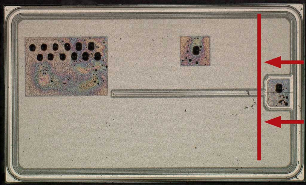
Figure 1: Entire die with the mechanical cross section location shown by the red line
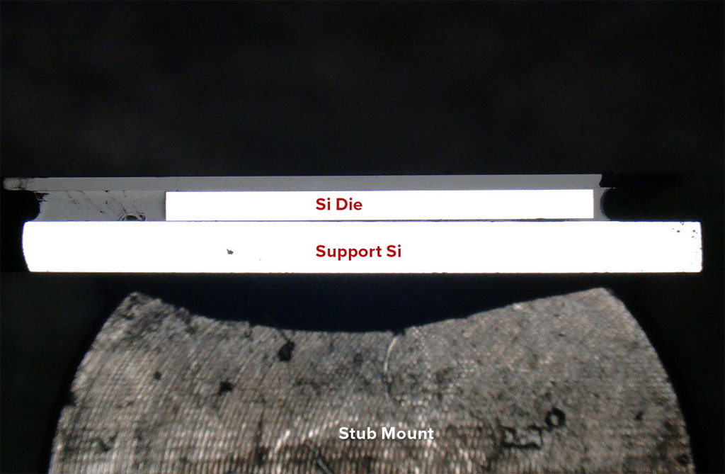
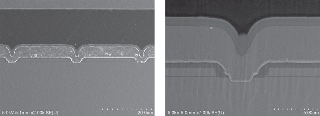
Figure 2: Mechanical x-section across whole die: side view of Figure 1 sectioned to the red line
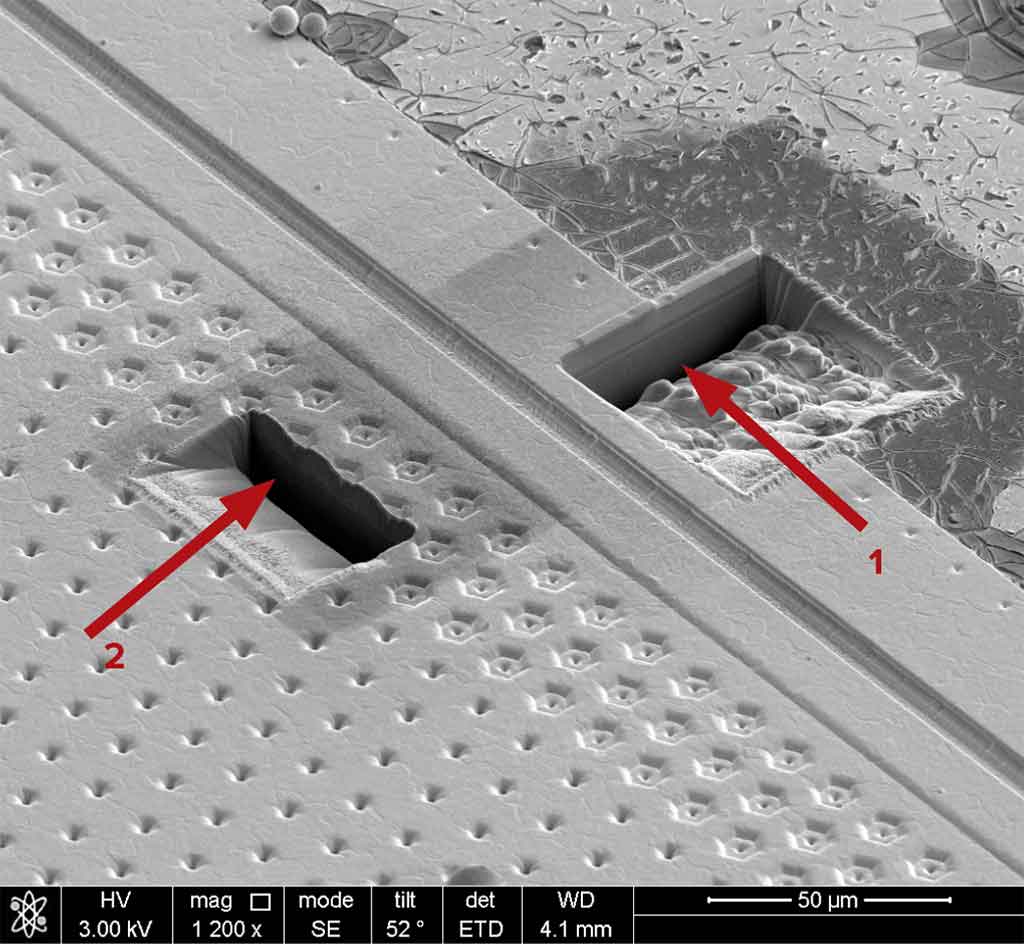
Figure 3: Trench 1 on the right is in the gate area and Trench 2 is in the Source field. The red arrow points to the section faces. The interior of each trench is imaged by the SEM on the instrument that is part of the dual beam FIB
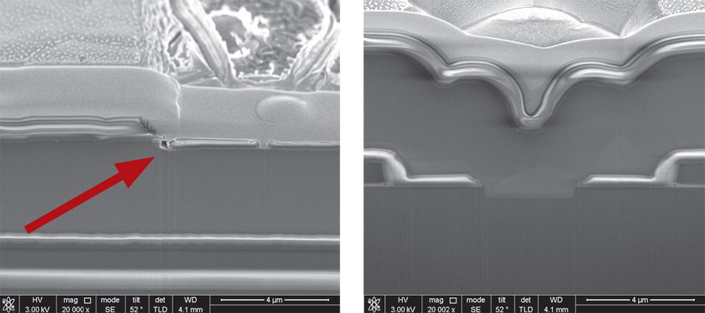
Figures 4 and 5: show the interior of the trenches, 1 and 2, respectively. Crack in oxide with a defect below at red arrow location
ADVANTAGES AND DISADVANTAGES
Mechanical sections have the advantage of spanning across the entire die (or package) allowing inspection at any point(s) across the sample. The sections can be additionally modified by wet etch or ion milling which increase the definition of layers or areas such as oxides or doped regions.
The exposed area can also be analyzed not only by optical microscopy and SEM but also techniques such as Scanning Capacitance Microscopy (SCM), micro probing, Fourier Transform Infrared (FTIR), hardness testing and others. This is due to the exposed nature of the section.
The disadvantages of the mechanical sections include: the application of pressure onto the sample which can cause cracking in brittle materials and fill in voids/cracks in soft materials, the ability to make controlled steps further into the sample is severely limited, the skill of the person performing the section bears heavily on the quality of the section.
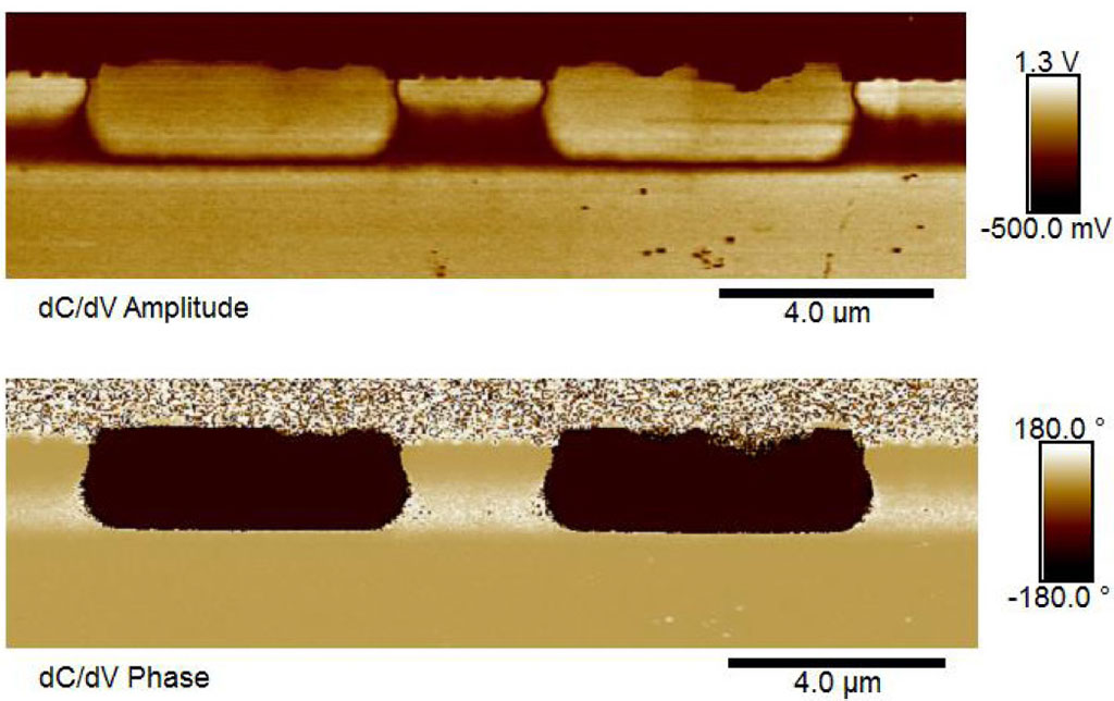
Figure 6: Top: SCM dC/dV amplitude image which shows relative dopant levels and Bottom: SCM dC/dV phase image which displays the dopant type distribution (brown = n type and yellow = p type)
A chemical wet etch was applied to the sample shown below to show the effect of this type of decoration. Note the appearance of the grain boundaries (red arrow) and the highlighted oxide layers were not clear after purely mechanical sectioning. The etch used depends on the sample material and what is desired to highlight: oxide, n or p doped regions in silicon.
Figures 7 and 8: SEM images of semiconductor die by mechanical x-section
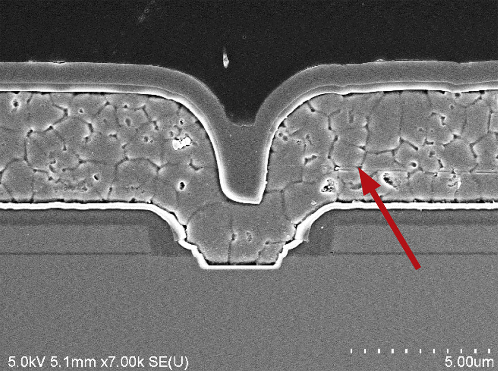
Figure 9: Mechanical cross section with decorative wet etch (note the enhancement of the grain boundaries compared to Figure 8)
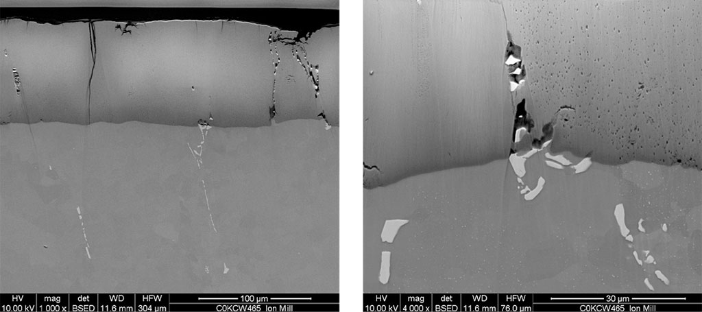
Ion milling can be applied to a mechanical x-section to clean up a portion of the section or ion milling can be done from the start for samples whose geometry allows. The ion milling gives a cleaner section than mechanical x-section. It also does not apply pressure to the sample which means brittle materials like GaAs, GaN and others section without the micro cracks common for mechanical sections.
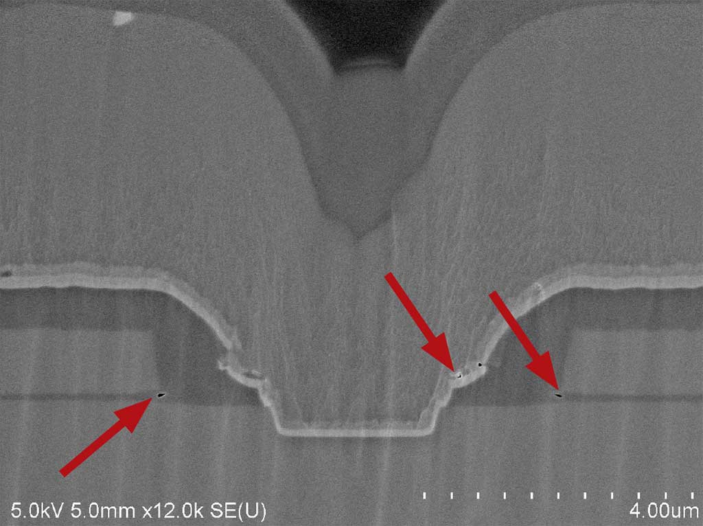
Also, soft materials like gold, indium or polymers are removed without filling in small voids or cracks on the sample, compare Figures 8 and 9 and note the appearance of several small voids on the ion milled sample. Ion milling can however introduce some artifacts, note the vertical streaks that show the milling direction. These can be reduced and even eliminated with careful set up and calibration of the ion milling tool.
Figure 10: Mechanical section followed with ion mill. Note small voids now visible (red arrows) For non-semiconductor materials the ion milling is best for maintaining small pores and other effects subject to change with mechanical sections and on too large a scale for FIB
Figures 11 and 12: Small voids and materials show up well in this ion milled ANO over Al
One limitation of ion-milling is that the area of interest must be at the edge of the sample. Additionally, the depth into the sample is limited – generally to 1.5 mm across and 700 microns into the sample depending on the instrument (more expensive tools can mill larger areas). Ion mills may be purchased with cryo-stages and other accessories that allow smearable materials like some polymers to be sectioned without redistributing the material.
The DB-FIB can reasonably cut a trench 20 microns across and 10 microns deep as a standard operation, including the imaging. The great advantage of DB FIB is that the section can be moved in a very controlled manner a very small distance into the sample. For example, 20 steps of 0.1 micron each can be made into the sections (Figures 4 and 5) to walk through an area of interest. Each of the steps can be imaged, analyzed by EDX and eventually made into a movie. Mechanical x-sections cannot be controlled in so fine a degree.
The disadvantages of DB-FIB are primarily the limited area exposed and the difficulty working with non-conductive samples. DB-FIB does not allow inspection across the entire die but does permit imaging of key locations, which can be very close to one another and at varying angles (see Figure 3). The small areas exposed exclude DB-FIB from serious consideration when looking at packaging issues such as solder ball/bump attach across a device.
The issue of charging is very serious when working on insulating samples and makes this a poor choice for these samples.
The limited area of the DB FIB section and the geometry of the hole make staining by wet etch very difficult and additional techniques cannot access the section.
The major advantages and disadvantages of each method are summarized in the table below:
Method
Advantages
Disadvantages
Mechanical X-section
Whole die/package can be inspected. Access for additional techniques is good.
Cannot take small controlled steps further into the device, pressure is applied to the sample.
Ion Milling
Very clean polish, no force applied to device. Grain structure can be observed. Uses noble gas to mill so no contamination issues.
Sample geometry is restricted, limited depth of section from sample edge.
Dual Beam FIB
Small controlled steps can be taken through the area of interest, multiple adjacent areas can be analyzed. Very easy to progress to TEM sample.
Only a small area is analyzed, limited depth of cut, large areas cannot reasonably be analyzed. Access for additional techniques is very limited. Uses Ga ions to sputter and this can be an issue. Has same charging issues for insulators as SEM.
SUMMARY
The decision on which type of cross section is best for a sample depends on the sample itself and the information that is needed. This paper addresses the most common technical advantages and disadvantages of each method: mechanical, ion milling and Dual Beam FIB, as they apply to most samples, especially for semiconductor applications. Each method has advantages and disadvantages and it is important to know the limitations and capabilities of each. Some of the methods discussed allow additional work while others do not: a die that has FIB cuts can then be mechanically sectioned, or moved on to TEM work, but a mechanical section is usually encapsulated prior to sectioning and no FIB work is then possible. Ion milling requires the area of interest to be at the edge of the sample which may require the sample to be prepared by cleaving or prior mechanical polishing. So, the order of operations can also be important. Most important to all analytical work is a good discussion and planning before the first operation is made.
REFERENCES
J. Devaney, G. Hill, R. Seippel, Failure Analysis Mechanisms, Techniques, and Photo Atlas, Failure Recognition and Training Services, Inc. 1986, Section 8.
The Microelectronic Failure Analysis Desk Reference, 3rd Edition, eds. T. W. Lee, and S. V. Pabbisetty, ASM International, 1993, pp. 97-110.
Failure Analysis Techniques – A Procedural Guide, eds. E. Doyle Jr. and B. Morris, IITRI, 1980, Section III-N.
J.C.H. Phang, D.S.H. Chan, S.L. Tan, W.B. Len, K.H. Yim, L.S. Koh, C.M. Chua, L.J. Balk, “A review of near infrared photon emission microscopy and spectroscopy”, Physical and Failure Analysis of Integrated Circuits 2005. IPFA 2005. Proceedings of the 12th International Symposium on the, pp. 275-281, 2005.
Act Quah, Ls Koh, Cm Chua, M Palaniappan, Jm Chin, Jch Phang, “DC-Coupled Laser Induced Detection System for Fault Localization in Microelectronic Failure Analysis”, Physical and Failure Analysis of Integrated Circuits 2006. 13th International Symposium on the, pp. 327-332, 2006.
P. Lawrence, “The Dualbeam (FIB/SEM) and its Applications – Nanoscale Sample Preparation and Modification,” 2006 19th International Vacuum Nanoelectronics Conference, Guilin, 2006, pp. 127-128. doi: 10.1109/IVNC.2006.335390
Y. Chuang, C. Huang, J. Hsu and Y. Wu, “GaAs device two-steps junction stain and scanning capacitance microscopy sample preparation,” 2017 IEEE 19th Electronics Packaging Technology Conference (EPTC), Singapore, 2017, pp. 1-3. doi: 10.1109/EPTC.2017.8277565
Would you like to learn more about sample sectioning?
Contact us today for your sample sectioning needs. Please complete the form below to have an EAG expert contact you.
To enable certain features and improve your experience with us, this site stores cookies on your computer.
Please click Continue to provide your authorization and permanently remove this message.