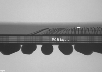
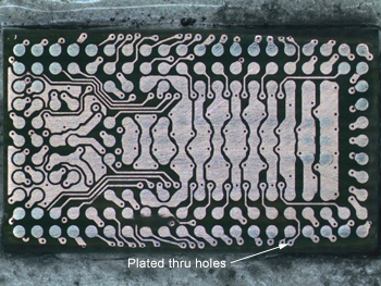
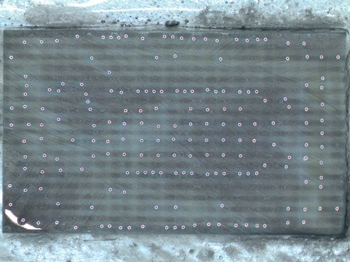
PCB or Package samples can be delayered and examined at each layer. Package delayering is helpful in looking for as well as design rule distances with in such samples. Packages can also be removed to allow analysis from the backside of die.
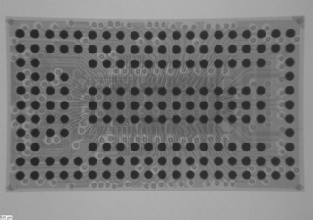
First a low mag X-ray is used to take a top view of a package. This is then repeated with the solder ball back, and sides
The device is then polished away layer by layer so that examination, images and analysis can be performed as needed.
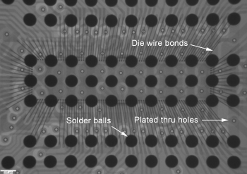
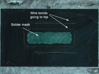
The exposure of the die and the wire bonds allows Emission/OBIRCH/IR techniques to be applied to the device.
View of stitch bonds that go to the top of the die surface
Would you like to learn more about Package Delayering Services?
Contact us today for your package delayering service needs. Please complete the form below to have an EAG expert contact you.
To enable certain features and improve your experience with us, this site stores cookies on your computer.
Please click Continue to provide your authorization and permanently remove this message.