Alkali Contamination in Thin Dielectric Films
Home » Alkali Contamination in Thin Dielectric Films
The performance of oxide and other dielectric layers in electronic devices can be compromised by low-level mobile-ion alkali contamination such as Li, Na and K. Dynamic SIMS depth-profiling measurements offer excellent detection limits (≈5E13/cm2) and accurate in-depth distributions for these contaminants. SIMS is therefore a powerful diagnostic tool and plays a key role in contamination reduction programs.
During a SIMS analysis these mobile species can drift to the oxide/substrate interface because a charged ion beam is used to profile the sample. Accurate charge compensation is of paramount importance during the analysis in order to obtain the correct concentration and depth distribution of the mobile ions in complex dielectric structures. Figure 1 shows SIMS profiles of Na in a borophosphosilicate glass (BPSG) film on a semiconductor device. Both Na profiles show moderately good charge compensation in that no appreciable Na has migrated to the BPSG/Si interface (700nm). However, the blue curve (non-optimized charge compensation) appears to show a diffusion of Na from the interface at 100nm (deposition interruption at this point) into the BPSG layer.
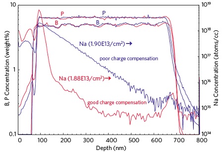
This may mislead one as to the mechanism by which the Na is being incorporated into the BPSG. The correct Na profile, in red, shows that, in fact, very little Na is actually incorporated into the BPSG. Virtually all of the Na is retained at the deposition-interruption interface at 100nm. A small Na peak is still detected at the BPSG/Si interface and this is undoubtedly a real contamination peak.
SURFACE EFFECTS OF STRAIN AND PLASMA ETCHING
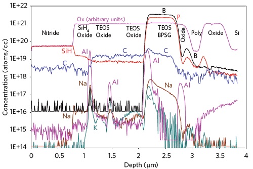
Figure 2 is a depth profile of Na, K, B, P, Al, C and O acquired in a single analysis on a device structure composed of SiN/SiO2/BPSG/SiO2/Poly-Si/SiO2/Si. Accurate quantification and in-depth distributions of the alkali elements allows one to determine exactly where in the process the mobile ions are being introduced into the layers. For instance, the correspondence between the presence of Na and K peaks with peaks for Al shows that the alkali contamination was introduced at the points in the process where the three Al metal I, metal II and metal III were deposited. An accurate SIMS profile of a device passivation layer can reveal many aspects of the dielectric process.
The C profile shows that the topmost SiO2 layer (0.8um to 1.1um) was deposited from a silane (SiH4) source while the higher levels in the next two layers show that these layers were deposited from a tetraethyl orthosilicate (TEOS) source.
The same SIMS analysis can also be used to measure and quantify the B and P in the BPSG layer in the layer stack.
Would you like to learn more about Alkali Contamination in Thin Dielectric Films?
Contact us today for your alkali contamination in thin dielectric film needs. Please complete the form below to have an EAG expert contact you.