Surface and Interface Characterization of Polymers
Home » Surface and Interface Characterization of Polymers
The surfaces and interfaces of polymer films impact many properties including adhesion, printability, barrier performance, appearance and strength.
WHY ARE SURFACES IMPORTANT?
Much of the value of converted polymer products revolves around surface modification and coatings. The thickness of these layers can range from the sub-nanometer – for contaminants or corona treatments – to tens of microns for packaging, paints and laminates.
WHAT TOOLS ARE AVAILABLE FOR STUDYING POLYMER SURFACES?
When questions arise about surface chemical properties of materials many of the commonly available analytical tools are poorly suited because their signals originate from the “bulk” of the polymer. Tools for probing the near-surfaces of materials fall into three broad categories with some overlaps. These categories include: (1) physical property testing, (2) microanalytical and, (3) surface chemical.
Physical property testing techniques include contact angle (for surface energy), micro- and nano-mechanical testing and optical tools such as ellipsometry.
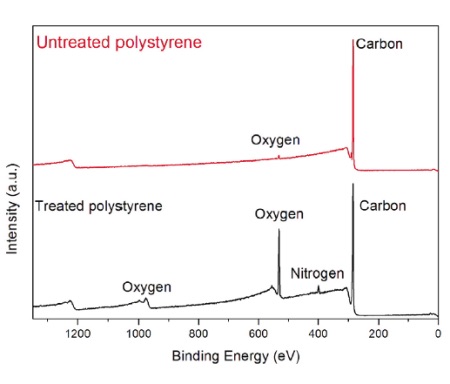
Figure 1 X-ray Photoelectron spectra of untreated and plasma treated polystyrene showing evidence of O and N on the treated film
Microanalytical tools include optical, electron (both scanning and transmission) and scanning probe techniques such as atomic force microscopy (AFM). Of these, the scanning probe microscopies are the most surface sensitive, obtaining their signal from the outer <1nm in most modes. The sampling depth of the low energy secondary electrons detected in SEM is a few nm while backscattered electrons come from 10-100 nm and X-rays – the basis for energy dispersive x-ray spectroscopy (EDS) – may come from more than 1 µm below the surface.
This paper will provide an overview of X-ray photoelectron spectroscopy (XPS) and time-of-flight secondary ion mass spectrometry (TOF-SIMS). These two tools are arguably the most powerful analytical techniques available for probing the chemical structure of polymer surfaces and interfaces. Case studies from polymer films will be discussed to demonstrate these capabilities. An exciting recent innovation that extends the reach of these tools beyond the top few nm will be introduced.
PRINCIPLE OF XPS
In XPS, which is also known as Electron Spectroscopy for Chemical Analysis (ESCA), a photon ionizes an atom resulting in the ejection of a core electron. The kinetic energy, KE, of these photoelectrons is related to the x-ray source energy, hν, by the photoelectric effect:
KE = hν – BE Eqn (1)
where BE is the binding energy of the core electron. Since each element in the periodic table has a different electronic configuration, XPS can be used to identify the elements present in a sample. The number of emitted photoelectrons is proportional the concentration of that element present within the sample, by way of near-universal sensitivity factors, making the technique quantitative without standards. Most commercial instruments use soft x-ray sources with hν<1500 eV resulting in photoelectrons with kinetic energies in the 200-1400 eV range. Electrons in this energy range travel only a very short distance through solids making the technique inherently surface sensitive; virtually all the signal originates from the outer 5-10 nm of the sample. Somewhat analogous to NMR, XPS has the ability to determine the nearest neighbor chemical environment in many organic and inorganic materials by way of small changes (termed “chemical shifts”) in the energy of the photoelectrons.
Figure 1 shows typical X-ray photoelectron spectra of an untreated and plasma treated polystyrene. The photoelectron peaks show up at discrete energies reflective of the energy at which they were originally bound to the nucleus. The untreated sample contained primarily carbon with only a small contribution (~1%) from oxygen. [Note that hydrogen is not detected in XPS.]
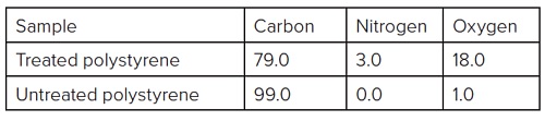
Table 1 Summary of elements detected on treated and untreated polystyrene (units are in atomic %)
After plasma treatment a significant oxygen peak and a small nitrogen peak are evident. The intensity of the photoelectron peaks are converted to concentration by using relative sensitivity factors that normalize for the different probabilities of producing the photoelectron for a different shell and getting the electron out of the solid.
Table 1 summarizes the elemental composition for the spectra in Figure 1.
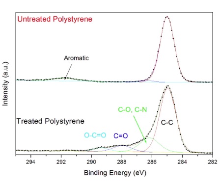
Information about the chemical functional groups is obtained from high energy resolution spectra acquired from the carbon energy range (Figure 2). The untreated polystyrene (top) contains only CHx bonds at 285 eV and a weak band due to aromatic bonds at 292 eV.
The plasma treated sample contains a series of bands due to CHx, C-O, C-N, C=O and O-C=O functional groups. The amount of each functional group is quantified by mathematically fitting the peak with a series of symmetric bands. This example of a plasma treated polystyrene surface highlights the four main attributes of XPS:
surface sensitivity (1-10nm sampling depth),
elemental and chemical state identification,
quantitative without the use of standards
ability to examine highly insulating samples.
Figure 2 High resolution carbon 1s spectra of untreated and plasma treated polystyrene showing C- O, C-N, C=O and O-C=O functional groups on the treated film
PRINCIPLE OF TOF-SIMS
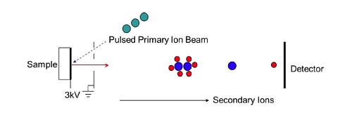
Figure 3 Schematic of a TOF-SIMS experiment showing lighter ions reaching a detector before heavier ions do thus separating them by the time it takes them to fly to the detector
In a time-of-flight SIMS experiment a very short (10-12nsec) pulse of primary ions strikes a sample creating a pulse of positive and negative ions as well as neutral fragments. The ions are subjected to an extraction field Ve of several thousand volts (Figure 3). This imparts each ion with a fixed kinetic energy, Ek, given by Ek = qVe, where q is the ion charge which is typically 1. The kinetic energy can also be expressed as Ek = ½ m v2 where m is the mass of the ion and v is its velocity. Since the kinetic energy is the same for all ions the velocity of each ion will be inversely proportional to its mass. By allowing the accelerated ions to fly through a field-free tube and then measuring their arrival time at a detector at the end of the flight tube, the ion’s mass can be calculated. Hence, a TOF-SIMS spectrometer requires a pulsed ion source, an extraction field, a flight tube, and a detector capable of detecting the arrival of each individual ion.
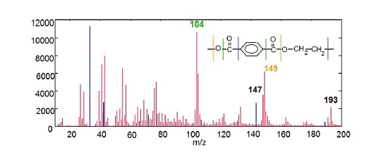
Figure 4 shows a positive ion mass spectrum collected from the surface of a polyethylene terephthalate film with a polydimethyl siloxane (PDMS) surface contaminant. The mass spectrum contains many fragments that can be used to identify the PET. PDMS fragments (shown in blue) are: Si (28), SiCH3 (43), SiC3H9 (73), Si2C5H15O (147).
The mass spectrum is acquired from a localized area (~1µm on an insulator). The incident ion beam is scanned in an XY pattern on the sample surface similar to a scanning electron microscope. Individual mass spectra are acquired from each position (typically a 256 X 256 array). Each of the more than 65,000 pixels acquired contains a high mass resolution spectrum from a given region on the sample. The mass spectra from any series of pixels may be summed and examined. Alternatively, the intensity of specific mass peaks may be displayed as a function of position.
Figure 4 Positive ion TOF mass spectrum of polydimethyl siloxane contaminated polyethylene terephthalate. PDMS peaks are shown in blue for clarity include: Si+, SiCH3+, SiC3H9+ and Si2C5H15O+
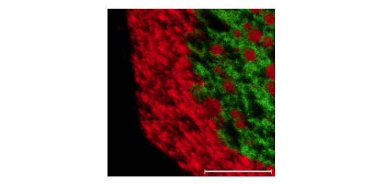
Figure 5 TOF chemical map showing organic molecule (green) and Mg (red) distribution on a surface
Figure 5 shows a 250µm X 250µm TOF image of an organic molecule (green) and an inorganic additive (red).
The main attributes of TOF-SIMS are:
surface sensitivity (<0.5 nm sampling depth),
elemental and molecular identification,
ability to chemically map elements/molecules on a surface with <1µm image resolution
ability to examine highly insulating samples.
This paper will show case studies where the unique attributes of XPS and TOF-SIMS are used to solve surface-related problems in the polymer and coatings industries.
CASE STUDY #1: IDENTIFICATION OF DEFECTS ON METALLIZED POLYMER-PSA LAMINATE
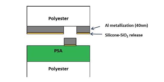
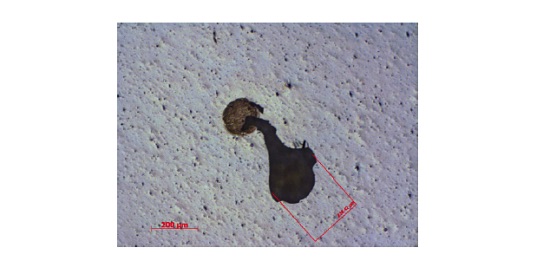
A laminate consisting of an acrylic-based pressure sensitive adhesive (PSA) on a polyester film bonded to a metallized PET with a silicone release layer experienced isolated defects that were 50-200µm in size. The defects resulted in the undesirable transfer of the metallization to the PSA surface. A schematic of the laminate is shown below (Figure 6) along with an optical micrograph of a defect (Figure 7). In cases of adhesion failure it is desirable to examine mating sides since the contaminants may preferentially transfer to one surface. Analyzing both sides of a failure can also help confirm the locus of failure which is not always straightforward in multilayer laminates containing transparent materials. Small area XPS was performed on mating sides of a 200µm defect.
Figure 6 Schematic of defects in PSA-metallized polyester sample
Figure 7 Optical micrograph of defect
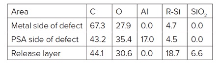
Species detected on the void defect on the metal side of the failure included: CHx, C-O, O-C=O and silicones. The data were consistent with PET, covered with 1-2 monolayers of silicone. The surrounding area was a silicone release material so there was concern that silicone had migrated to the defect surface post failure.
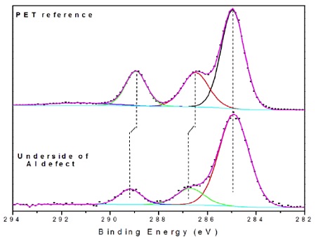
The PSA side of the failure (i.e., underside of Al flake) contained Al, Al2O3, CHx, C-O, O-C=O and silicones (Table 2). The locus of failure was quite clearly at the polyester-Al interface. A closer look at the carbon spectrum on the underside of the Al flake revealed C-O and O-C=O peaks of equal intensity. This is an indication of the presence of an ester while the only organic species should have been a small amount of -CH3 from the silicone and any airborne organic picked up post failure.
Transfer of PET to the metal was considered, but there were subtle clues in the high resolution spectrum that this ester was from an aliphatic ester, not an aromatic polyester like PET (Figure 8)1. Specifically, the distances between the CHx and C-O and between the CHx and O-C=O bands were 0.25-0.30 eV larger on the defect than on a PET reference sample. Such shifts are consistent with the presence of an aliphatic ester present on surface of the PET prior to metallization. This caused the adhesion failure of the film.
Figure 8 High resolution C 1s spectra from defect (bottom) and a PET reference (top) showing shifts in the binding energies of the C-O and O-C=O. There is also no evidence of the weak aromatic band at ~292 eV on the defect
Figure 6 Schematic of defects in PSA-metallized polyester sample
CASE STUDY #2: FAILED HEAT SEAL
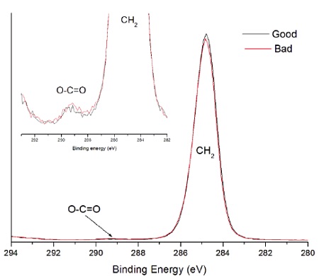
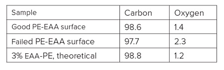
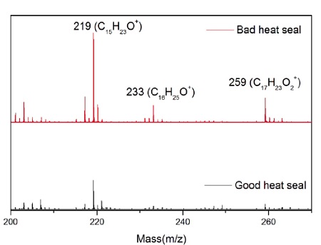
A sterile package from a medical device experienced adhesion failure at a polyethylene-ethylene acrylic acid (co-polymer) heat seal to polyethylene interface. EAA added at 3% improves adhesions and results in a lower % of crystallinity. Good and bad heat seal surfaces were examined using XPS and TOF-SIMS. XPS found only carbon and oxygen on the surfaces. The high resolution carbon spectra are overlaid in Figure 9. The inset confirms the presence of a small amount of O-C=O as expected from the acrylic acid species. If we assume that all the oxygen comes from EAA, the Good heat seal contains the expected 3% amount of EAA, but the Bad heat seal contains closer to 5% EAA (Table 3). TOF-SIMS was performed on the surfaces to try to confirm the presence of higher EAA. Both surfaces contained ions indicative of PE (C2H3, C3H5, C4H7, etc.) and EAA (CH3O, C2H5O, etc.). However, the bad heat seal also contained intense peaks for a hydroxyhydrocinnamate compound (Figure 10). Such compounds are common antioxidants under the Irganox® brand.
Figure 9 High resolution photoemission spectra of good and bad heat seal surface. Inset shows weak O-C=O expected for EAA
Table 3 XPS results from Good and Bad Heat Seal
Figure 10 Positive ion mass spectra for good (lower) and bad (upper) heat seal showing more intense hydroxyhydrocinnamate ions at 219, 233 and 259 amu for the bad seal.
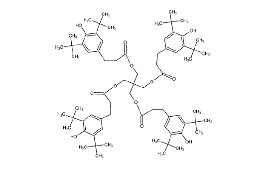
Figure 11 shows the molecule for Irganox® 1010, one of the common hydroxyhydrocinnamate compounds. Weak hydroxyhydrocinnamate peaks were observed on the Good heat seal surface at roughly 1/3 the intensity.
XPS was only able to identify an alkyl carbon and a weak O-C=O band. In this case, the EAA-PE co-polymer and hydroxyhydrocinnamate contaminants contained these same species making it impossible for XPS to identify the contaminant. The quantitative nature of XPS did allow it to detect higher O levels on the bad seal.
The molecular specificity of TOF-SIMS showed that the excess oxygen did not come from EAA, rather there were elevated levels of an antioxidant on the heat seal surface. It was concluded that this was the root cause of the adhesion failure.
Figure 11 Irganox 1010 molecule
WHAT ABOUT BURIED LAYERS AND INTERFACES?
Accessing exposed surfaces by directly sampling them or through delamination is straightforward with XPS and TOF-SIMS. However, many polymer systems contain laminated layers where the surface or layer of interest may be buried many microns below the top surface in a system that cannot be easily failed. Historically, the main choice for investigating systems like this was to section the laminate and examine it in cross section using a micro-focused technique like FTIR, Raman, SEM-EDS or TOF-SIMS. This is generally best done on soft materials using a microtome. In these cases the lateral resolution of the technique limits the thickness of the buried layer or interface that can be probed. For FTIR the resolution is ~15µm while for SEM-EDS, Raman and TOF-SIMS it is ~1µm. The relatively poor lateral resolution of XPS (20-30µm) limits the application of XPS on cross sectioned polymers.
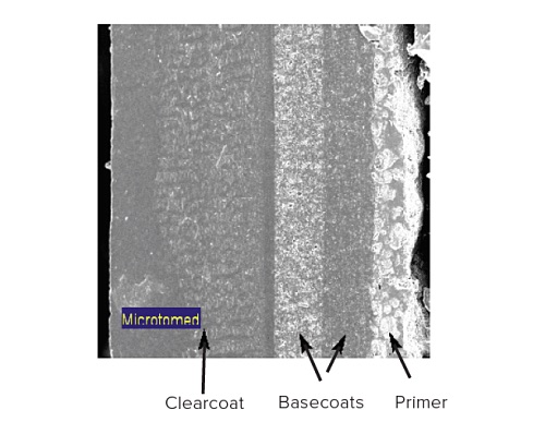
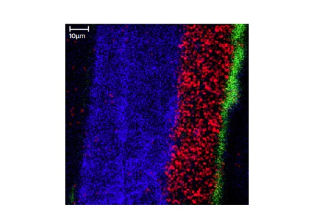
Figure 12 shows a SEM image taken from a cross-sectioned paint sample. This painted sample contains a substrate (not shown), a primer layer, two basecoats and a clear coat. Since the layers of interest are all greater than 5µm TOF-SIMS can be used to chemically image the different layers (Figure 13).
Figure 12 SEM image from a microtome sectioned paint sample
Figure 13 Chemical image of paint cross section. Green= Fe from primer corrosion; Red = Al & Ti from basecoats; Blue = Cl from clearcoat
WHAT ABOUT LAYERS AND INTERFACES THAT ARE < 1µm THICK?
For buried layers and interfaces in inorganic multi-layer systems it has long been possible to sputter from the top surface through the various layers and expose buried interfaces with a high degree of control using monatomic ion beams of argon, oxygen, cesium, gallium or even gold. Numerous factors can affect the measurement, but resolving buried layers that are only a few nm in thickness is fairly common, especially with SIMS. Until recently, the same was not possible on organic systems. The process of monatomic sputtering leads to bond breakage, cross linking, gas evolution and various other damaging events that render the remaining surface unrecognizable to XPS and TOF-SIMS. After several tens of nm of sputtering most polymers resemble amorphous carbon and thus only limited chemical information can be obtained.
However, in the last decade and a half a new kind of ion beam has been developed that offers the hope of being able to sputter into organic systems and maintain the chemical state information which is so essential to analyzing polymer systems. These ion beams involve polyatomic clusters of atoms and, as such, are called gas cluster ion beam (GCIBs).
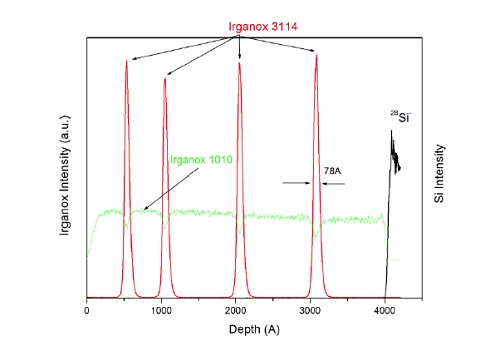
Figure 14 Molecular depth profile acquired using Ar cluster GCIB source on multilayer organic thin film sample
The first broadly available cluster beam was Buckminsterfullerene, C60. As these C60 clusters impact a surface, the kinetic energy of the projectile is divided among the 60 carbon atoms resulting in much less damage to many polymeric systems. EAG has the newest generation of GCIB which utilizes ~10,000 Ar atoms loosely held together via Van der Waals forces. This Ar cluster beam technology has revolutionized TOF-SIMS and XPS by allowing these techniques to extend their reach beyond the top 1-10nm.
Figure 14 shows a molecular depth profile of a specially designed test specimen made from alternating thin and thick organic layers deposited on a silicon wafer.
TOF-SIMS with GCIB profiling is able to maintain the molecular signal from the two different Irganox molecules as a function of depth. This capability can be extended microns to 10s of microns into organic coating systems.
SUMMARY
XPS is a surface sensitive analytical tool for probing chemical phenomena on polymer surfaces. Standardless quantification, ability to identify not only what elements are present on a surface, but also the chemical state of those elements makes XPS a powerful tool for characterizing polymer surfaces and interfaces. TOF-SIMS offers two complementary attributes to XPS: (1) determination of specific organic compounds present on a surface (rather than simply the functional groups) and (2) chemical mapping with ~1 µm resolution. Combined, these tools provide the most complete chemical analysis of polymer surfaces and interfaces. With recent advances in ion beam technology the capabilities of XPS and TOF-SIMS can now be extended beyond the top surface opening a new realm of characterization opportunities on multilayer polymeric systems.
1. G. Beamson and D. Briggs High Resolution XPS of Organic Polymers John Wiley & Sons (Chichester) 1992.
Would you like to learn more about Surface Characterization of Polymers?
Contact us today for your surface and interface characterization of polymer needs. Please complete the form below to have an EAG expert contact you.
To enable certain features and improve your experience with us, this site stores cookies on your computer.
Please click Continue to provide your authorization and permanently remove this message.