Nanoindentation (NI)
Home » Our Techniques » Spectroscopy » Nanoindentation
Nanoindentation (NI) is a nano-mechanical test that provides the mechanical properties from precise compliance measurements. In addition, nanoindentation analysis is especially useful in measuring properties such as the modulus and hardness of various shaped and sized materials. For example, nanoindentation is useful to characterize semiconductor thin films, packaging, advanced alloys, thermal barrier coatings, polymer viscoelasticity, scratch and wear resistance.
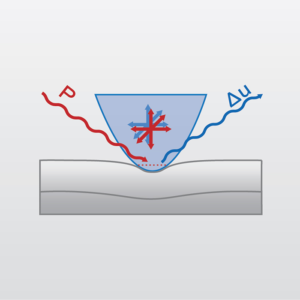
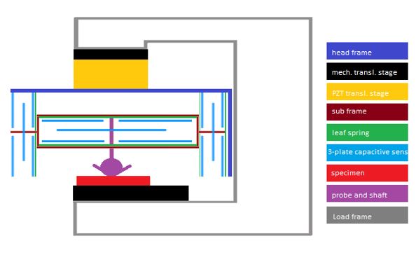
Nanoindentation uses contacts, where a probe is pushed into a solid, while the penetration depth is recorded simultaneously with near-atomic resolution. In addition, this capability can reduce the probing volume down to an order of magnitude of 100 nm3, which allows the use of continuum mechanical contact models to extract properties like hardness and modulus for thin films and constituents of microstructures. The contact geometries and testing methods are configurable so that mechanical characterization can be extended to brittle properties, adhesion, stress-strain, scratch, wear or structural stiffness of microstructures.
Theory of instrumented-indentation
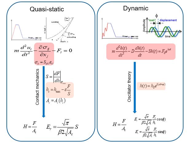
Nanoindentation experiments are typically conducted either quasi-statically or dynamically, while the properties are extracted using contact or oscillator physics.
Examples of Nanoindentation
- Firstly, a quick assessment of wafers or thin films on wafers during quality control
- Investigation of effects during process development (e.g. PVD, CVD) in semiconductor device fabrication
- Simulation of contact conditions observable in practical use-cases for failure analysis
- Mapping spatial distribution of mechanical characteristics on multi-phase materials
- Studying deformation mechanisms (elasticity, plasticity, brittle behavior or phase-transformation)
- Accurate assessment of structural compliance of microstructures and particles
- Gaining highly localized insights into stress-strain relationship of a material
- Studying adhesion properties on surface and thin film interfaces
- Obtaining accurate mechanical property values for input into physical modeling (e.g. finite element or analytical analysis)
- Lastly, an assessment of viscous material properties through creep and relaxation testing, as well as dynamical mechanical analysis on the nanoscale
Ideal Uses of Nanoindentation
- Firstly, quantitative mechanical characterization of highly-localized material properties, including hardness, elastic modulus, fracture toughness, creep, topography
- Secondly, obtaining other material characteristics, including storage- and loss-modulus from dynamic mechanical analysis (DMA) on nano-scale, thin film adhesion, wear, friction and structural compliance
Advanced Loading Techniques
Firstly, quasi-static indentation:
Secondly, dynamic indentation:
Thirdly, nano-scratch:
Finally, in-situ imaging:
- Trapezoid
- Multiple partial unloading
- Stiction
- Creep
- Grid
Secondly, dynamic indentation:
- Variable load
- Variable frequency
- Continuous stiffness
- Modulus mapping
Thirdly, nano-scratch:
- Constant load
- Progressive load
- Tilt corrected multi-pass
Finally, in-situ imaging:
- Contact mode
- (Scanning-) wear
Strengths
- Accurate test positioning on features of few-100 nm size
- Quantitative characterization of thin films
- Wafers up to 6 in analyzed intact
- Dry and liquid environment
- Cross-section analysis (including in-house preparation)
- Numerous non-indentation applications, which are solely custom-designed around precise control and measurement of force and displacement in mixed-load-conditions at small scales
Limitations
- Firstly, bulk specimen size limitations 4x2x2 inches
- Secondly, thin film measurements under 10 nm thickness should be considered semi-quantitative
- Finally, potential problems with extremely rough surfaces
Nanoindentation Technical Specifications
- Control modes: Force, Displacement
- Useable Min./Max. Load: <5 nN / >10 mN
- Useable Noise-floor/Max. Displacement: <0.1 nm / >20 μm
- Controllable oscillator drive frequency: 1 – 300 Hz
- Specimen holders: Vacuum, Magnetic, Gravity, mechanical clamping
- Probes: Conical, Flat, Berkovich, Cube, custom sizes and shapes
- Lateral Resolution: <50 nm
Related Resources
In conclusion, nanoindentation is a great tool to investigate many mechanical properties of a material.
Would you like to learn more about using Nanoindentation (NI)?
Contact us today for your Nanoindentation (NI) needs. Please complete the form below to have an EAG expert contact you.