Electron Beam Induced Current (EBIC)
Home » Our Techniques » Imaging » EBIC
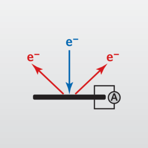
EBIC (Electron Beam Induced Current) is a scanning electron microscope (SEM)-based technique utilized for semiconductor devices. Like Cathodoluminescence (CL), the technique depends on the creation of electron-hole pairs (EHPs) by the high energy electron beam of the SEM to create the analytical signal. EBIC utilizes a sensitive pico-ammeter connected between the p and n sides of the device to measure the resulting current, or EBIC, that flows as the electron beam is scanned across the sample in either plan-view (PV) or cross-section (XS). The intensity of the EBIC signal then corresponds to the strength of the built-in electric field around the p-n junction. Defects that act as recombination sites show significantly lower EBIC signal.
Typically, both EBIC and Secondary Electron (SE) signals are captured simultaneously, providing complimentary spatial maps of EBIC along with topographical and/or compositional information. EBIC is a very effective technique for locating otherwise hidden electrically active defects in large area (mm2) devices with 50-100 nm precision for further root cause failure analysis (FA) such as plan-view (PV), cross-sectional (XS) SEM or Scanning Transmission Electron Microscopy (STEM).
Additionally, Electron Beam Induced Current can be utilized to quantitatively determine the vertical location of a p-n junction within a complex heteroepitaxial structure such as the ones found in Light Emitting Diodes (LEDs), Vertical Cavity Surface Emitting Laser (VCSEL)s and Edge Emitting Lasers. In some cases, estimates of the minority carrier diffusion lengths can also be calculated from the same quantitative XS-EBIC data.
Ideal Uses of EBIC
- Semiconductor failure analysis – defect localization for deep FA
- Device characterization – junction location and minority carrier diffusion length
Strengths
- Great at finding otherwise hidden localized failure sites in large area devices
- Determination of p-n junction location in XS
Limitations
- A p-n junction must be present in the sample
- Acceptable maximum leakage currents are on the order of 10uA, otherwise EBIC data may be too noisy for usable analysis
EBIC Technical Specifications
- Signals Detected: Electron Beam Induced Current (EBIC)
- Imaging/Mapping: Yes
- Lateral Resolution: Typically varies from 20-500 nm depending on SEM conditions and sample composition/topology
Related Resources
Would you like to learn more about using Electron Beam Induced Current (EBIC)?
Contact us today for your Electron Beam Induced Current (EBIC) needs. Please complete the form below to have an EAG expert contact you.