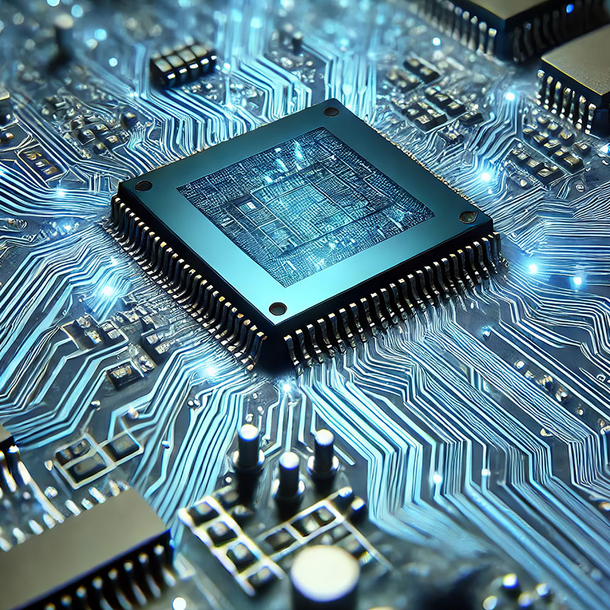
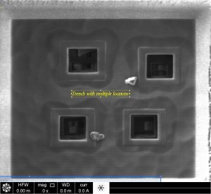
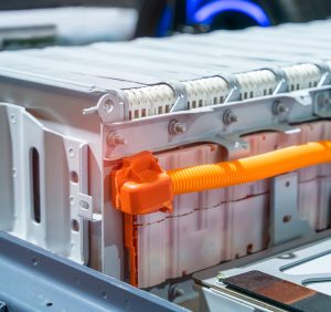
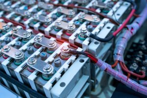
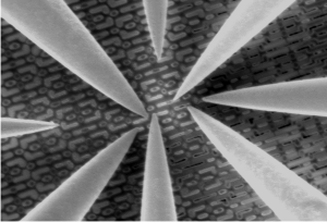
A Deep Dive into Dynamic SIMS vs. static-SIMS
Different types of SIMS analyses exist. The two main types include Dynamic SIMS (high current) and static-SIMS (low current).
Home » Blog
Different types of SIMS analyses exist. The two main types include Dynamic SIMS (high current) and static-SIMS (low current).
TEM, STEM and AC-STEM techniques deliver high resolution images providing a detailed view of a material or product.
Cryo FIB uses a cold sample stage that can be controlled to -135°C making it it more suitable for temperature sensitive materials.
RBS is the one technique where we can really say that the composition and concentration are accurately determined for thin films.
Gallium oxide has the potential to replace or substitute gallium nitride for power conversion in electric trains and vehicles.
Aerospace Materials Testing for Tunnel Junction Solar Cells Science has opened many doors in its advancement over the centuries.
Solids fall under two main categories: amorphous and crystalline. These two types of solids have different properties that may be more beneficial for certain products or applications.
Televisions, computer screens, cell phone screens etc. are getting clearer, sharper, brighter and use much less power. This is all possible through LEDs.
The elemental purity of boron carbide can be measured using several methods offered by Eurofins EAG Laboratories
Our laboratories in France and the Netherlands offer materials testing for industries including semiconductor, consumer electronics, lighting, aerospace and healthcare.
SEM-Cathodoluminescence is used for a wide variety of luminescent materials and devices. It allows for the inspection of optical properties with sub-um spatial resolutions combined with SEM imaging having 3-5nm spatial resolution.
One way to combat rising fuel costs in the aerospace industry and improve efficiency is to use new advanced materials such as Ceramic Matrix Composites (CMCs).
Besides images provided by SEM and TEM, different attachments can be added to reveal crystalline information, including (SEM-EBSD) and TEM (TEM-PED).
An injection molded component in a consumer product was found to have an increased failure rate over a three-month period.
A client requested assistance to investigate a recurrent issue with the curing failure of a silicone adhesive joint between metal components.
A client wanted to investigate the delamination of food packaging multilayer laminate. Roll stock did not meet seal strength specification.
EAG Laboratories provides clients with answers to these questions and more with testing support for every stage of the supply chain.
The Dual Beam FIB-SEM integrates a focused ion beam with a scanning electron microscope for simultaneous sample prepping and imaging.
The roughness of a surface and how it interacts with surrounding materials and elements can have a significant impact on material technology and its functionality.
XRF is a non-destructive technique that is used to quantify the elemental composition of materials.
EAG Scientists utilize GDMS analysis to perform Elemental Depth Profiling for chemical purity evaluations for aerospace & defense.
A company was investigating environmental stress cracking of polycarbonate components used in a conveyor device that was sanitized.
All materials have trapped gasses inside. Learn how EAG utilizes Evolved Gas Analysis to analyze what gasses are being released.
In the aerospace industry, electronics are subjected to extreme environmental variables. EAG’s failure analysis group can help solve potential problems that may arise.
As medical devices become more complex, there are many more opportunities for things to go awry. Identifying, diagnosing, and remedying failures becomes dramatically more challenging. We can help.
FIB Circuit Edit provides the ability to quickly perform nano-surgury by cutting traces or adding metal connections at the chip level
EAG Laboratories pursues quality in all aspects of our work for customers. ISO certifications and ongoing audits serves many market sectors.
FTIR and Raman are spectroscopy techniques that provide molecular information from various types of materials.
III-V materials partially provide us with the ever evolving and changing technological advances we enjoy today.
APT is a nanoscale materials analysis technique that provides 3D spatial imaging and chemical composition measurements with high sensitivity simultaneously.
A device manufacturer observed defects in a lot of thermoplastic tubing. The tubing exhibited signs chemical attack or exposure to heating.
High reliability electronic components like integrated circuits are often required to operate for long periods of time, having little or no opportunity for replacement.
Ion-exchanged glass is used in a variety of applications where strength, durability, and resistance to damage are important. Applications like smartphone screens.
Surface cleanliness is critical in how a material or a layer on a product interacts with other surfaces, which in turn can affect its functionality.
EAG scientists are leaders in the lithium-ion batteries recycling arena. EAG is a valuable resource in understanding these materials.
Eurofins EAG Laboratories stands ready to assist in the analysis of lithium-ion batteries from the raw material supply chain through to the finished product and eventual recycling.
EAG’s material and microelectronic testing service is dedicated to providing the best information from ensuring the purity of starting materials, to prototype testing of devices in the ramp up towards full-scale production.
Unwanted chemical impurities can be problematic. GDMS is a powerful full survey analysis tool for chemical purity evaluations.
EAG divides FA tasks into three levels. In each level, we employ optimal techniques for device characterization, defect localization, and root cause failure analysis.
Cracks were observed in transparent thermoformed plastic packaging during visual quality checks. Failures occured in specific material lots.
Developing a reliable product has many challenges due to the desire for increased capability, reduction in formfactor, and managing the supply chain.
Analytical testing to support changes in raw materials and processing conditions used in manufacturing memory foam, as well as odor
PFIB differs from traditional FIB in that it uses various gases such as Xe, Ar, oxygen or nitrogen to generate a plasma that is used to remove material from a sample.
Blisters were observed in paint applied to steel plates that had undergone treatment with a corrosion inhibitor. An investigation was performed to determine if there was evidence of contamination on the inside of the blister.
To be hermetically sealed essentially means to be airtight so that nothing can come in or get out (i.e., gas, moisture, liquid, etc.).
Atomic Layer Deposition technology aids in the demand for computational advancement in the microelectronics industry.
PCOR-SIMS was originally developed to analyze Silicon Germanium (SiGe) devices for the communications industry.
VCSELs have several advantages, such as a higher modulation speed, which make them great for technological innovations.
There is still so much to learn about batteries, including challenges such as energy density, cycle life, fast charge, and safety. In this blog, we’ll be focusing on energy density.
LA-ICP-MS is a technique that uses direct micro-scale sampling to provide high precision elemental characterization of solid materials.
Lithium-ion batteries provide high energy density mobile power but come with three challenges: performance, safety and battery life.
ICP-MS is a multi-elemental bulk chemical analysis technique that can determine simultaneously up to 70 elements in a single sample.
High Depth Resolution Analysis will play a very important role in the electronic device industry as devices become smaller and smaller.
Polymeric films used in an outdoor application experienced reduced adhesion over time. The client suspected that UV degradation was occurring.
EDS and EELS can be coupled with SEM, STEM and TEM to determine the elemental composition, spatial distribution and segregation of elements.
In our interconnected and changing world, it is important to know how to respond to potential electronic system failures.
Cryo TEM involves performing TEM analysis while keeping the sample at cryogenic temperatures, around -170°C.
To enable certain features and improve your experience with us, this site stores cookies on your computer. Please click Continue to provide your authorization and permanently remove this message.
To find out more, please see our privacy policy.