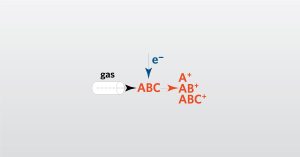
The Power of SEM-EDS in Imaging and Elemental Analysis

SEM (Scanning Electron Microscope) equipped with EDS (Energy Dispersive X-ray Spectrometer) can capture detailed images and identify elements simultaneously on the surface of samples. For imaging, SEM is widely used since it needs minimal sample preparation and produces excellent resolution, unique contrast, and a large depth of field. When paired with an EDS system, elemental information of the imaged area can also be derived. SEM-EDS is ideal for imaging and elemental analysis applications requiring higher resolution than optical microscopy and identifying elemental make up. In SEM, an image is formed by scanning a focused electron beam, usually with energies of 1 to 20 keV, across a sample and detecting the ejected secondary or backscattered electrons.  The incident electron beam, when imparting energy to the sample, can cause emission of x-rays that are characteristic of the sample atoms. The energies of the x-rays are characterized using EDS to identify the elements in the sample. The typical spatial resolution of SEM imaging is about 5-10 nanometers.  SEM-based EDS is primarily a qualitative technique providing data from about a micrometer in diameter and a micrometer deep.

KWZ_0979-216

The strengths of SEM-EDS lie in its ability to provide rapid, high-resolution imaging, and enabling quick identification of elements present. Its excellent depth of field and versatility as a platform supporting various tools make it a valuable asset. Common applications include the failure analysis of integrated circuits, process development of submicron films, and features for optics, photovoltaic, semiconductor, biotechnology, and other industries. SEM-EDS is also employed in the characterization of metal corrosion, elemental identification of particles and process residues, investigation of interfacial layers, oxidization, and contamination. Additionally, it proves useful in imaging surface topography, including pits, scratches, and bumps. For imaging and analysis with sub-surface features, additional sample preparation methods such as chemical etching, mechanical cross-sectioning, planar polishing, and ion beam techniques are also available.

Battery Analysis using SEM-EDS

A customer approached us seeking to examine the elemental composition of a battery structure to pinpoint and understand materials, contaminants, or impurities affecting its performance. EAG conducted a thorough investigation using cross-sectional analysis with mechanical polishing, revealing intricate internal structures like the anode, separator, and cathode. The utilization of SEM-EDS enabled a comprehensive characterization of both spatial and chemical distributions of elements.

SEM-EDS at EAG

EAG has more than 25 SEM systems, including advanced tools like high-resolution field emission instruments, high-voltage tools (30 keV in SEM and 200 keV in STEM), and those operating in “Environmental” mode with a higher vacuum pressure. Our equipment can handle 300 mm wafers, and we have over 15 focused ion beam-SEMs (Dual Beams). We offer diverse sample preparation methods, from mechanical to various ion beam techniques.

In addition to our cutting-edge hardware, EAG has a skilled team of over 25 individuals experienced in SEM operations, ranging from Ph.D.’s and FAB process managers to metallurgy specialists. Our labs cater to various industries, including semiconductors, medical devices, optics, energy storage, cell phones, piping, and printing. Reach out to us to explore how our expertise and advanced tools can contribute to the success of your project.

More content you might like...

XRD

XRD Webinar

In this webinar we introduce X-ray Diffraction (XRD) which is a analytical technique for the examination of crystalline materials.

Read More »

To enable certain features and improve your experience with us, this site stores cookies on your computer. Please click Continue to provide your authorization and permanently remove this message.

To find out more, please see our privacy policy.