Advanced Microscopy
Home » Services » Materials Testing & Analysis » Advanced Microscopy Services
Advanced microscopy techniques such as SEM (Scanning Electron Microscopy), TEM (Transmission Electron Microscopy) and Dual Beam SEM are essential techniques to investigate sample microstructure, morphology, particle size, particle coatings and defects.
These techniques often employ elemental mapping capabilities such as EELS (Electron Energy Loss Spectroscopy) and EDS (Energy Dispersive X-Ray Spectroscopy), which provide valuable information about elemental composition and location/distribution.
EAG offers a broad range and large installed base of different microscopy tools and services to match your application, ranging from process development to failure analysis. In addition to providing high resolution imaging, our analytical capability makes us a unique partner that can help you during research, development, and analysis of failures.
WHY EAG for Advanced Microscopy Services?
EAG Laboratories provides the specialized support and services you need to accelerate time to market, fill equipment and expertise gaps, and manage risk associated with product development.
- Sample prep and analysis of wide range of materials
- Expertise in failure analysis with advanced product technologies
- Wide range of instruments and expert staff to handle complex projects
- Quick turn around with accurate analysis and data you can count on
We have a broad range and large installed base of different microscopy tools and services to match your application, ranging from process development to failure analysis. In addition to providing high resolution imaging, our analytical capability makes us a unique partner that can help you during research, development, and analysis of failures. We can perform structural and cross-sectional analysis, elemental material analysis, and microanalysis with sub-nanometer spatial resolution.
Microscopy techniques include:
- Field Emission Scanning Electron Microscopy (FESEM)
- Transmission Electron Microscopy (TEM)
- Scanning Transmission Electron Microscopy (STEM)
- Aberration Corrected-STEM
- Dual Beam (FIB/SEM) imaging
- SEM – Energy Dispersive Spectroscopy (EDS)
- TEM – Energy Dispersive Spectroscopy (EDS)
- TEM – Electron Energy Loss Spectroscopy (EELS)
Transmission Electron Microscopy (TEM)
Transmission Electron Microscopy (TEM) and Scanning Transmission Electron Microscopy (STEM) are closely related techniques that use an electron beam to image the internal structure of a sample. High energy electrons, incident on ultra-thin samples allow for image resolutions that are on the order of 2Å. Compared to SEM, TEM and STEM have better spatial resolution and are capable of additional analytical measurements, but require significantly more sample preparation.
Although more time consuming than many other common analytical tools, the wealth of information available from TEM and STEM analyses is impressive. Not only can outstanding image resolution be obtained, it is also possible to characterize crystallographic phase, crystallographic orientation (by diffraction experiments), produce elemental maps (using EDS or EELS), and obtain images that highlight elemental contrast (dark field STEM mode). These can all be done from nm-sized areas that can be precisely located. STEM and TEM are the ultimate failure analysis tools for thin film and IC samples.
EAG also has Aberration Corrected-STEM instrument to provide the best available image resolution from a commercial independent microscopy service.
Scanning Electron Microscopy (SEM)
Scanning Electron Microscopy (SEM) provides high-resolution and large-depth-of-field images of the sample surface and near-surface. SEM is one of the most widely used analytical tools due to the extremely detailed images it can quickly provide. Coupled to an Energy Dispersive X-ray Spectroscopy (EDS) detector, SEM also offers elemental identification of nearly the entire periodic table.
SEM is used in cases where optical microscopy cannot provide sufficient image resolution or high enough magnification. Applications include failure analysis, dimensional analysis, process characterization, reverse engineering, and particle identification. Our highly skilled staff enables you to meet the desired outcomes. Person-to-person service ensures good communication of the results and their implications. Customers are often present during the analysis, enabling an immediate sharing of data, imaging and information.
Dual Beam FIB (DBFIB)
A Focused Ion Beam (FIB) instrument uses a finely focused ion beam to modify and image the sample of interest. FIB is chiefly used to create very precise cross sections of a sample for subsequent imaging via SEM, STEM or TEM. Additionally FIB imaging can be used to image a sample directly, detecting emitted electrons either from the ion or electron beam. The contrast mechanism for FIB is different than for SEM or S/TEM, so unique structural information can be obtained in some cases. A dual beam FIB/SEM integrates these two techniques into one tool, facilitating “cut and look” studies.
Sample Preparation
As a sample preparation tool, the FIB can accurately produce cross-sections of a sample that are impossible to create otherwise:
- FIB has revolutionized sample preparation for TEM samples, making it possible to identify sub-micron features and precisely prepare cross sections.
- FIB-prepared sections are used extensively in SEM microscopy, where the FIB preparation, SEM imaging, and elemental analysis can happen on the same multi-technique tool.
- FIB-prepared sections are also used in Auger Electron Spectroscopy to provide elemental identification of subsurface features quickly and precisely.
- It is an ideal tool for examining products with small, difficult-to-access features, such those found in the semiconductor industry and for sub-surface particle identification.
- It is a good option for products that are hard to cross section, such as soft polymers that are challenging to polish.
EAG works with a wide range of materials and regularly assists companies with FIB sample preparations and analyses. No other lab can match EAG’s skill set, experience, and fleet of instruments. Plus, you can count on fast turnaround times, accurate data, and person-to-person service, ensuring you understand the information that you receive.
Advanced Microscopy Examples
Microscopy techniques can be used to characterize many types of defects. These include:
- Metal migration: FIB cross-section and investigation by STEM/EDS
- Voids: FIB cross-section and investigation by SEM
- Particles: Surface imaging or FIB cross-section to investigate size, chemistry and position in the layer stack
- Cracks and Delaminations: Small area FIB cross-sections or large area argon ion milled cross sections determine the location and of the delaminated interface. If needed, the interface chemistry can then be determined by TEM micro-analysis.
- Thickness and Uniformity: FIB cross-section and investigation by SEM
The types of materials tested using advanced microscopy techniques:
- Nanoparticles
- Alloys and metals
- Thin films
- Coatings on glass, silicon or carbon-based substrates
- Ceramics
- Composite materials
- IC devices
- Aluminum anodization
Industrial Applications of Advanced Microscopy
There has been a rapid emergence of new technologies, which has enabled new industries such as facial recognition, autonomous driving, virtual reality, and 5G communication. These growth areas typically include FinFET, VCSEL, and III/V compound semiconductors. For our Advanced Microscopy team, the materials indicate hetero-epitaxy, cubic and hexagonal lattices, where failures in devices often have complicated 3D structures.
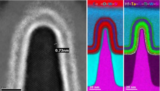
Recent development of FIB technology enables high-precision TEM sample preparation of 3D logic and memory devices. This example shows a HAADF image of a gate cut from a 22 nm generation 3D FinFET device with LGate~30 nm, as seen in a recent paper by the EAG Laboratories Advanced Microscopy team that was presented at Microscopy and Microanalysis 25 (S2): 690-691 (2019) “Industrial Applications of Electron Microscopy: A Shared Laboratory Perspective”
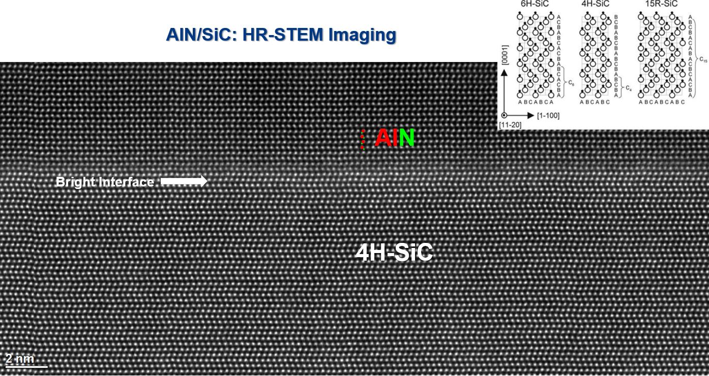
Another interesting example is the picture above that shows an aluminum nitride/silicon carbide interface observed using HR-STEM imaging.
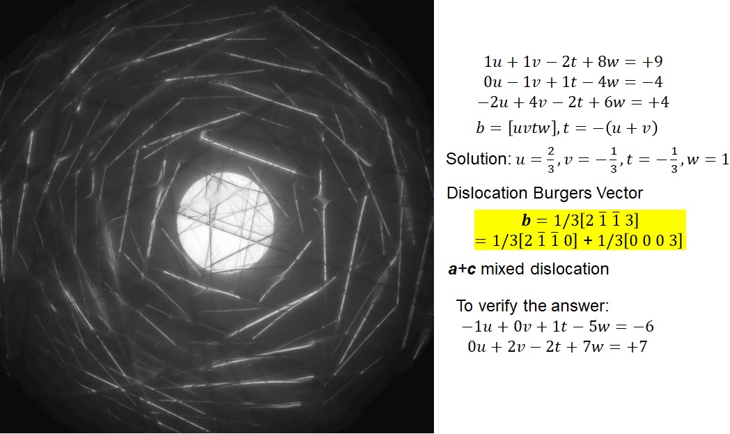
In this example above, we observe GaN Dislocation Typing: Burgers Vector Analysis with Large-Angle Convergent-Beam Electron Diffraction (LACBED)
Would you like to learn more about using Advanced Microscopy Services?
Contact us today for your Advanced Microscopy Services needs. Please complete the form below to have an EAG expert contact you.