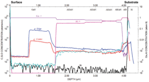
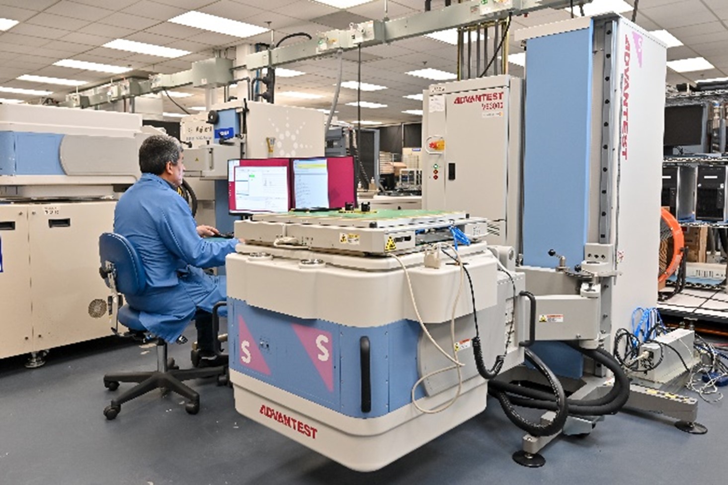
Using SIMS to Scrutinize HEMTs
HEMTs characterization using SIMS helps to uncover troublesome impurities, optimize epitaxial layer growth and aid failure analysis
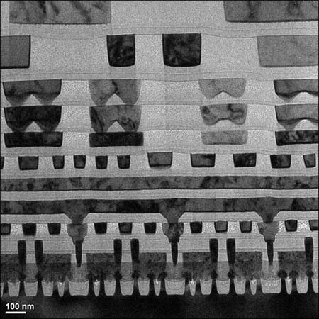
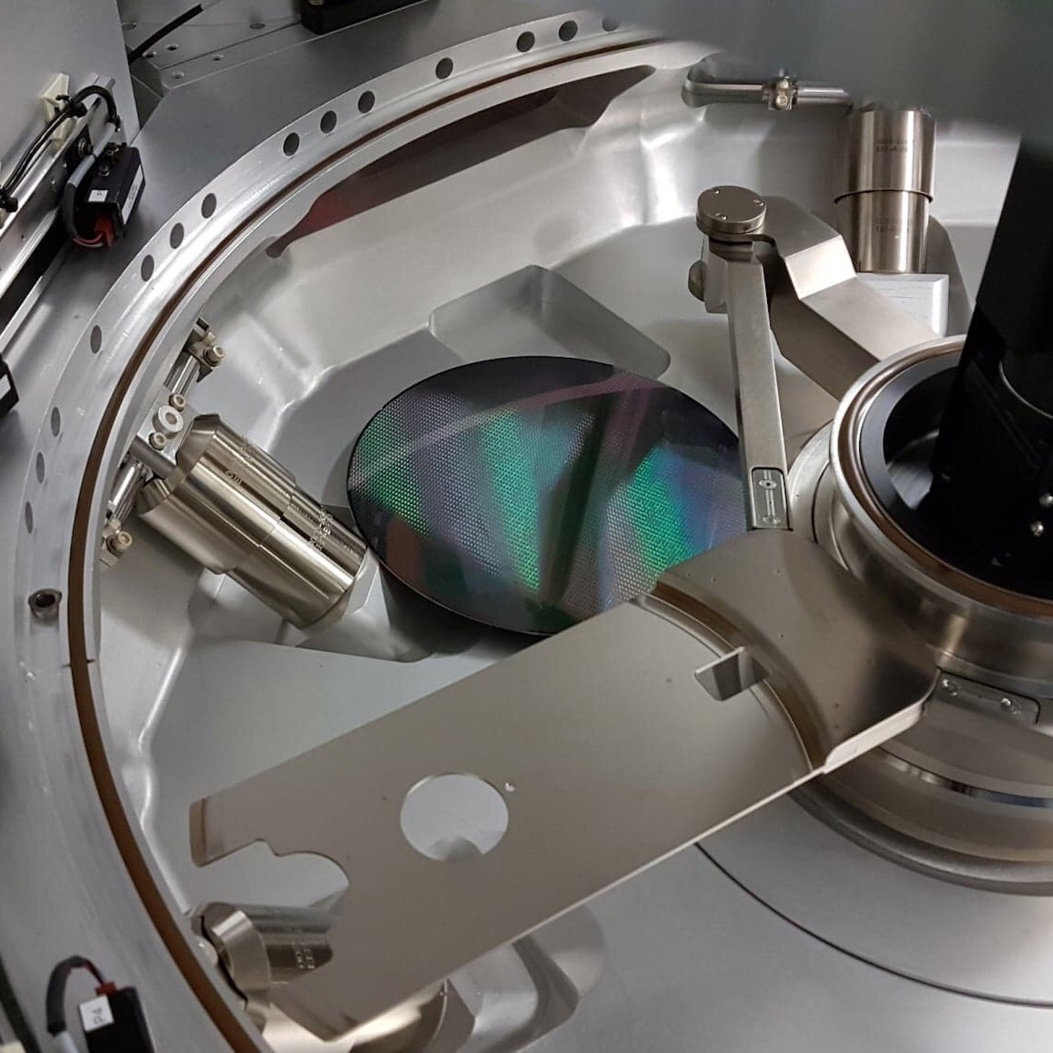
HEMTs characterization using SIMS helps to uncover troublesome impurities, optimize epitaxial layer growth and aid failure analysis

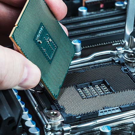
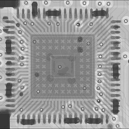
In this webinar we show how EAG troubleshoots electronic system failures using a multidisciplinary approach
February 12, 2025
During this live Ask the Expert event, we will answer pre-submitted questions from our audience regarding Silicon Carbide for High Powered Electronics. EAG Laboratories has a vast depth of experience analyzing silicon carbide using both bulk and spatially resolved analytic techniques and is the world-leading materials characterization and engineering resource for semiconductor testing.
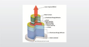
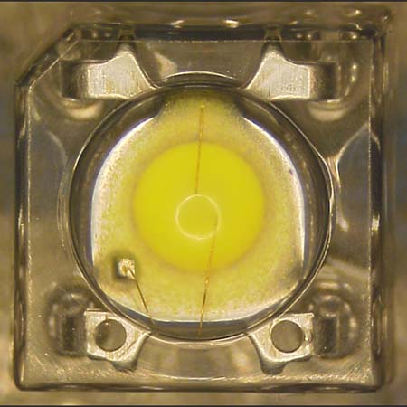
In the full webinar we will introduce analyzing VCSELs with a focus on secondary ion mass spectrometry (SIMS)
To enable certain features and improve your experience with us, this site stores cookies on your computer. Please click Continue to provide your authorization and permanently remove this message.
To find out more, please see our privacy policy.