Chemical Analysis of Plasma Resistant Ceramic Coatings
Home » Chemical Analysis of Plasma Resistant Ceramic Coatings
In the semiconductor industry in general and particularly in liquid crystal display (LCD) manufacturing, several processes involve plasma etch and plasma clean. The high-speed plasma stream can be extremely corrosive to manufacturing compartments and the surfaces that are exposed to the plasma resulting in formations of residual particles. Consequently, particles formed in chambers can contaminate substrates that are being processed, thus contributing to device defects. To minimize particle formations, plasma resistant ceramic coatings are required on various components exposed to plasma including the plasma etcher, the plasma cleaner, or the plasma propulsion system, such as the chamber walls, bases, gas distribution plates, rings, view ports, lids, nozzles, shower heads, substrate holding frames, electrostatic chucks, face plates, and selectivity modulation devices, among others.
Plasma resistant ceramic coatings under development or currently in active use, are typically multi-layered structures that provide plasma erosion resistance, rigidity, conformability to substrate and thermal shock resistance. Rare earth oxide, alumina, carbides, and nitrides based ceramic materials are currently used and/or under further developments. Coating precursors include ceramic powders, sintered ceramic solids, metal and metal alloy targets, and metal halides, depending on the component substrate materials, coating technique and application environment.
FULL SURVEY CHEMICAL ANALYSIS OF CERAMIC COATINGS
High resolution Glow Discharge Mass Spectrometry (GDMS) is recognized as one of the most versatile direct sampling techniques for survey chemical analysis of solids. The glow-discharge plasma source combined with high-resolution mass analyzer is suitable to evaluate mass fractions in solids directly and with very high sensitivity.
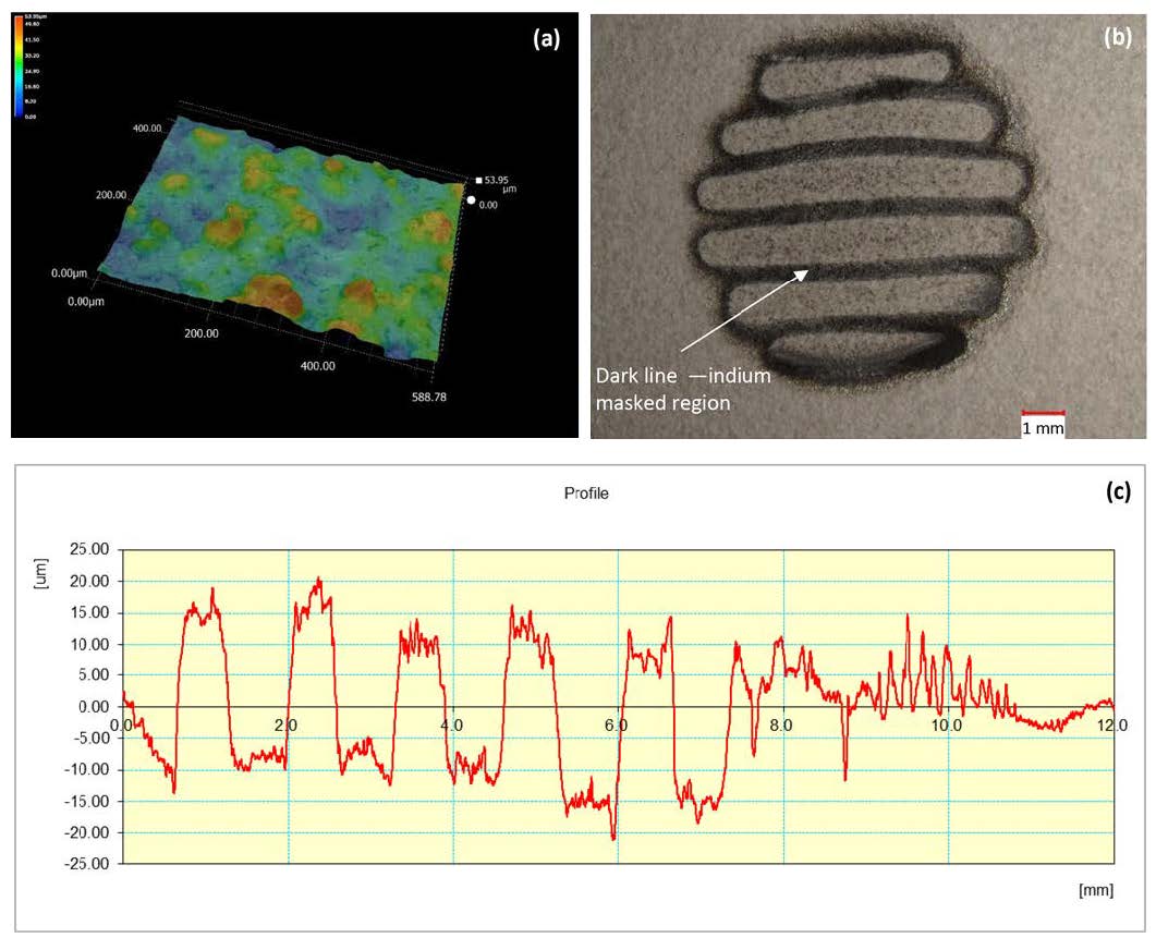
Figure 1 shows:
(a) 3D illustrations of a typical plasma resistant ceramic coating roughness;
(b) plasma atomized spots using indium mask with six sampling openings. Darker lines around the atomized spots are indium deposits on the surface from the mask; (c) plasma atomized crater cross-section profile. Sampling orifice diameter ~ Ф 10 mm; average sputtering depth ~ 20 μm.
Would you like to learn more about Analysis of Plasma Resistant Ceramic Coatings?
Contact us today for your analysis of plasma resistant ceramic coating needs. Please complete the form below to have an EAG expert contact you.