2D/3D realtime X-ray inspection solutions
As components get more complex, nondestructive inspection techniques like X-Ray and CT scanning help uncover issues and anomalies
Home » App Note

As components get more complex, nondestructive inspection techniques like X-Ray and CT scanning help uncover issues and anomalies
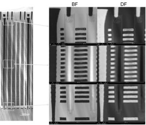
30keV Scanning Transmission Electron Microscopy (STEM) can provide 3Å resolution bright field (BF) and dark field (DF, ADF, HAADF) images
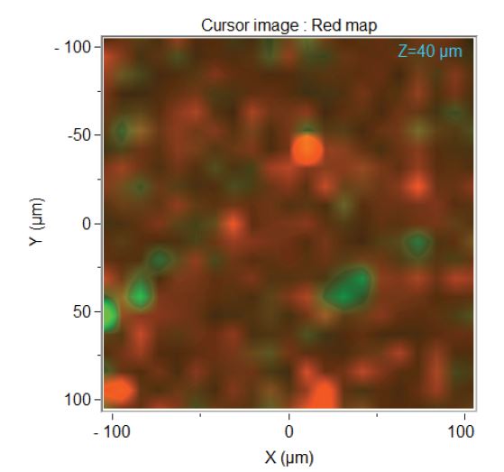
A very good use of Raman is for the analysis of pharmaceutical products to determine the spatial distribution of components of interest
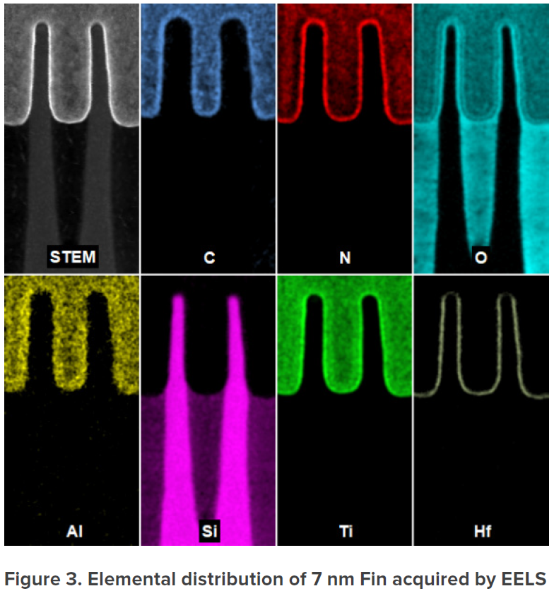
We provide a materials analysis study into the comparison between 22 nm node and 7 nm node FinFET technologies, using TEM-based techniques.
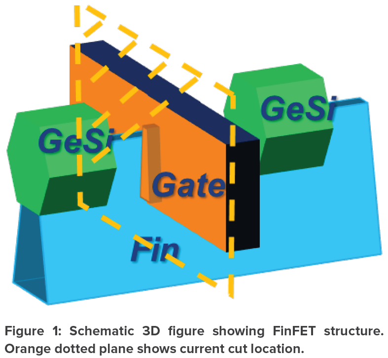
A study into the structure, elemental distribution and crystal orientation of a 22nm FinFET using TEM based analysis techniques
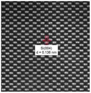
Aberration Corrected Scanning Transmission Electron Microscopy (AC-STEM) significantly improves the resolution of the traditional STEM tools.
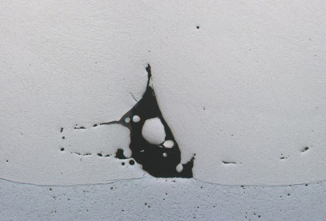
Additive manufacturing is transforming how products and parts are manufactured that in more cost-effective solution.
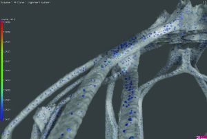
Additive Manufacturing (3D printing) enables the creation of products with freedom in design and choice of polymers, metals, and ceramics.
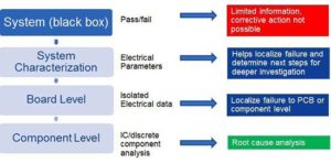
Electronic systems failure analysis methodology and workflow by applying FIB circuit edit techniques for solving electronic problems.
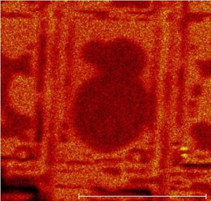
Advanced Surface Analysis using TOF-SIMS on a flat panel display, discovering residue formed during the manufacturing process.
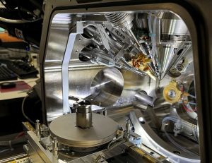
At Eurofins EAG Laboratories, we have utilized Plasma Focused Ion Beam (PFIB) to overcome the limitations of traditional deprocessing methods.
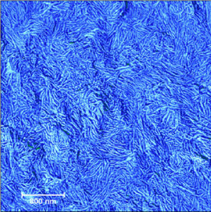
Polymer surface modification by Atomic Force Microscopy (AFM) for understanding surfaces of medical device polymers for biocompatibility.
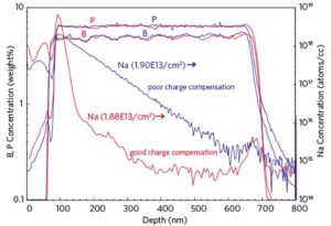
Alkali contamination can compromise performance of oxide and other dielectric layers in electronic devices.

Wavelength Dispersive X-Ray Fluorescence Spectroscopy (WDXRF) is an ideal analytical tool for determining or verifying alloy compositions

CIGS Thin Film PV performance reliability and uniformity as manufacturing is scaled up, can be optimized using materials characterization.
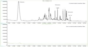
Thermal desorption GC/MS – Good vs. failed comparisons for detecting volatile organic components and for semi-quantitative results.
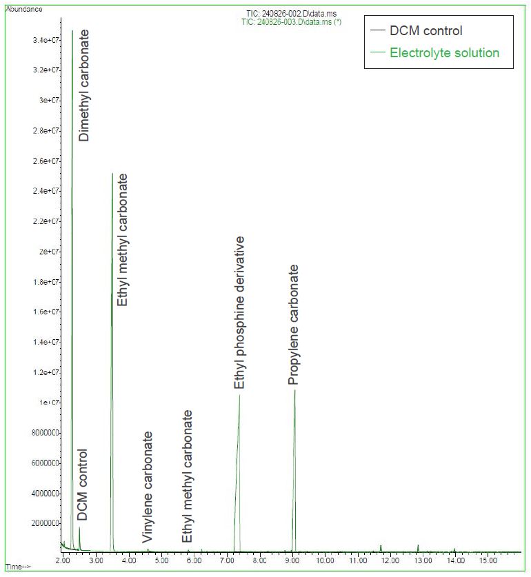
The GC-MS method offers a simple, reliable, and accurate approach for analyzing the composition of lithium-ion battery electrolytes and ensuring quality control.
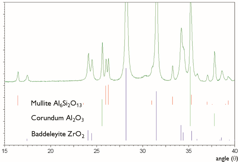
XRD and EDS analysis of refractory materials that are typically used in glass tank furnaces are zirconia, alumina and silica-based bricks.

Antifouling Paint Release Testing is a product chemistry specialty, to determine the release of biocides from marine paint coatings.
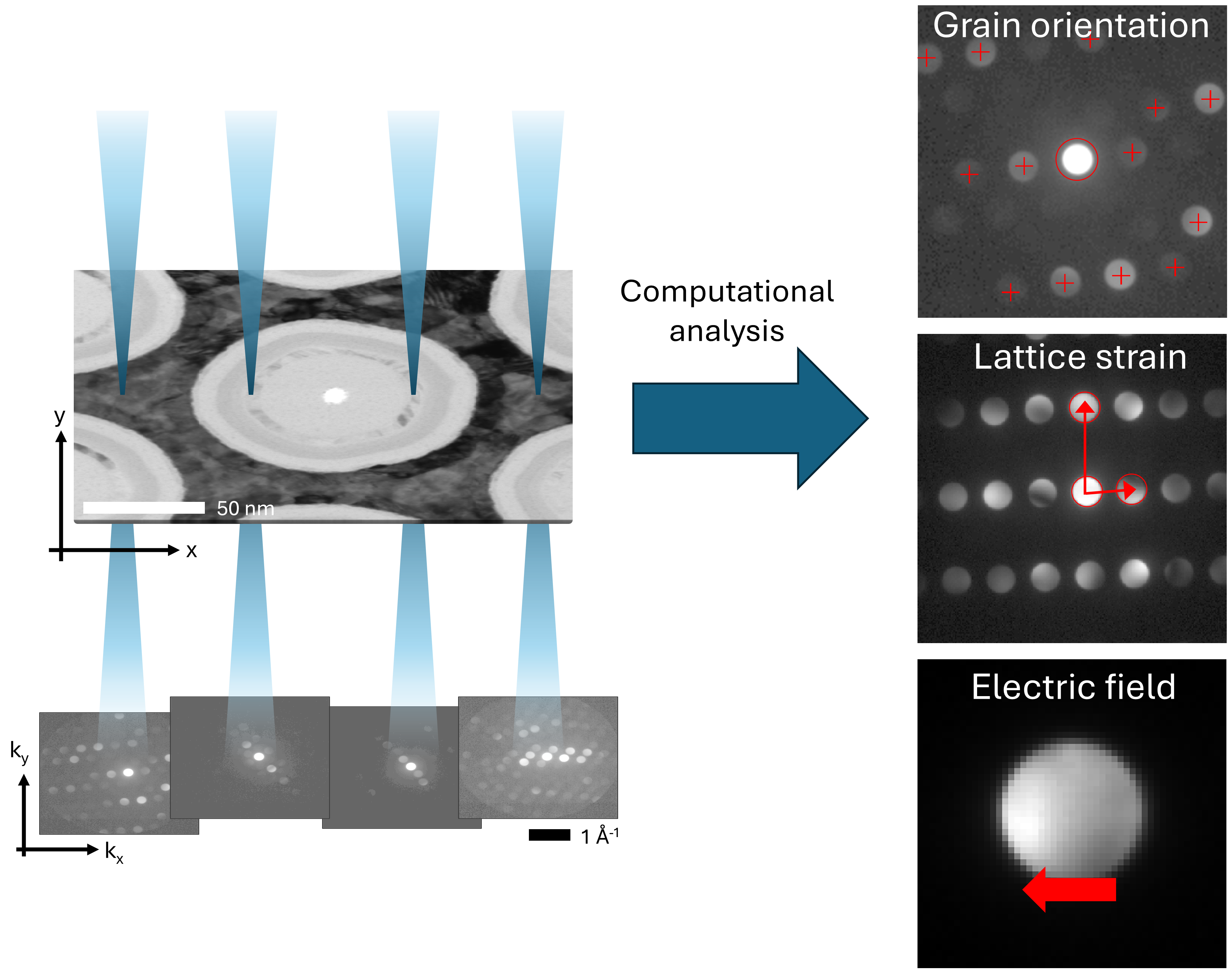
In this application note, we will focus on three applications of 4D-STEM: orientation mapping, strain analysis, and electric field imaging.
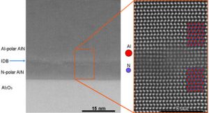
In this application note, we show how different signals obtained through AC-STEM can provide direct observation of local polarity switching.
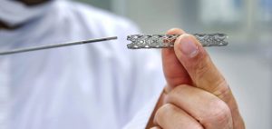
EAG evaluate corrosion and leaching of nickel-rich implanted medical devices including nitinol, stainless steel and MP35N.
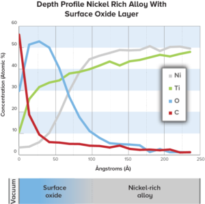
Nickel biocompatibility assessments of intravascular stents from EAG includes evaluating corrosion, surfaces and nickel ion release testing.
Our extensive list of test methods in our ASTM testing lab for paints, coatings, adhesives and plastic manufacturers.
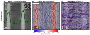
In this application note, we show the possibility to extract distance information at an atom-column to atom-column basis with picometer level precision.
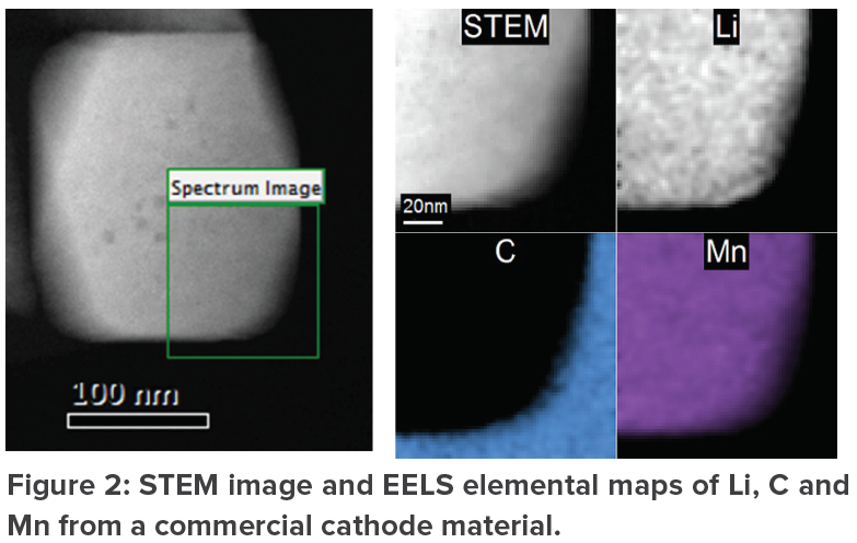
EELS and EDS coupled with STEM provides chemical composition along with structure information of materials.
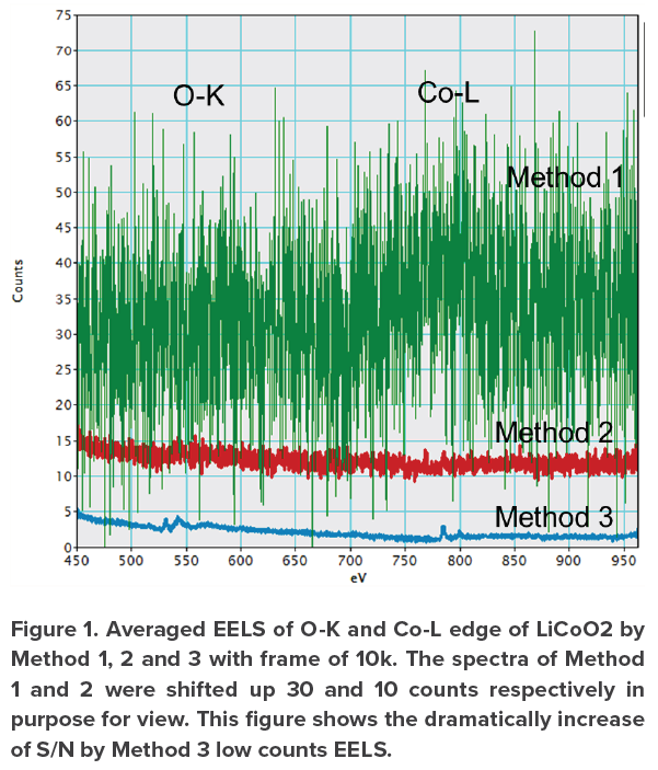
With the demand of lithium-ion batteries, it is critical to understand the structure and composition with high spatial resolution.
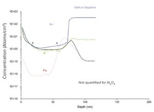
Atomic layer deposition analysis helps you meet ALD specifications for composition, thickness, and crystallinity.
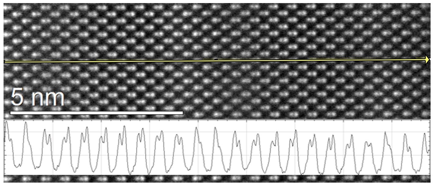
Advances in thin film growth has created a need for characterizing structure and chemistry at the atomic scale using EDS.
AC-STEM with Secondary Electron (SE) imaging provides the unique capability of evaluating specimen surface morphology with atomic-resolution.
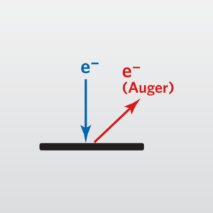
Auger Tutorial by EAG, in this instrumentation overview we present the history of Auger, along with details regarding analyzers and detectors
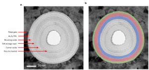
In this application note, we highlight how deep learning methods for image segmentation, such as convolutional neural networks (CNNs) or vision transformers, can help interpret the complex contrast of TEM images and segment a series of thin films in 3D NAND devices.

Eurofins EAG Laboratories is your partner for battery materials testing throughout the battery life cycle. From raw materials to product failures, we can provide the data needed to help you provide top quality and high-performance products to market faster.
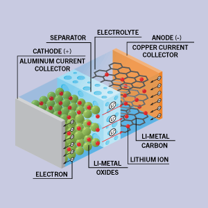
Assessing the chemical state of various components of a battery, from the cathode to the current collectors, at different stages of cycling, provides crucial insights into the electrochemical processes that occur during battery operation.

Battery Raw Materials Analysis Battery manufacturing is a meticulous process where the integrity and performance of the final product hinge on the purity of its

Battery recycling of key materials such as cobalt, nickel, and lithium require precise and accurate determination of elemental compositions
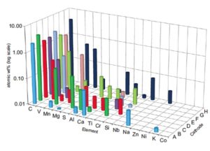
Battery materials characterization services includes analysis of raw materials, surface chemistry, composition, morphology and uniformity
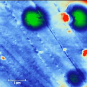
Atomic Force Microscopy, AFM imaging helps medical device manufacturers understand how coatings behave when applied to a medical device surface.

Biomedical Morphology and Microstructure through imaging analysis – characterizing crystallographic phase and producing elemental maps.
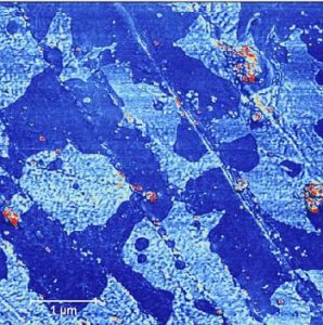
Biomedical products analyzed by EAG Laboratories include stents, catheters, balloons, implants, lens, diagnostics and more
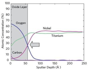
Biomedical surface analysis looks at properties critical to medical and pharmaceutical products, and offer answers to difficult problems.

Catheter and balloon analysis for medical device development support includes deformulation, contaminant identification and failure analysis.
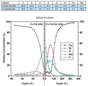
Laminate failure : Multi-layer laminate by analysis by XPS. Investigation details adhesive failure at a Ni2Mo-Cu interface due to monolayer contamination.
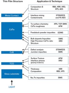
CdTe Thin Film PV manufacturers benefit from surface analysis techniques such as SIMS, GDMS, SEM,TEM to support efficiency improvements.
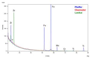
WDXRF and XRD are two powerful tools that allow us to obtain detailed characterization of materials, covering both the elemental composition and crystalline phases present.
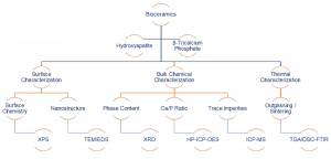
This paper will demonstrate how analytical tools can be used for the quality control of hydroxyapatite and β-tricalcium phosphate powders
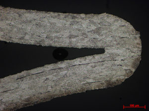
Stents characterization from EAG includes nitinol, stainless steel and MP35N. Experiences with fatigue resistance and hydrogen embrittlement.
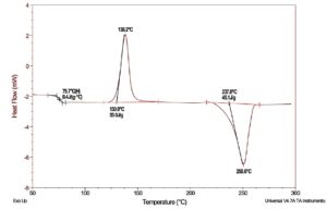
DSC analysis of polymers provides polymer characterization & thermal properties for product improvement and problem solving.
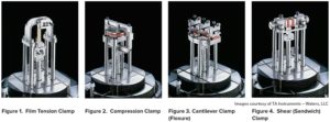
Polymeric materials characterization: Dynamic mechanical analysis (DMA) to study viscoelastic properties under conditions of low applied mechanical force.
Surface Aluminum Characterization highlights advantages of using SurfaceSIMS.XP to determine contamination on processed Si wafers.
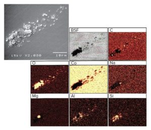
A discussion of EAG’s elemental characterization of defects and contamination on surfaces for failure analysis through EDS, SEM and AES.
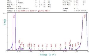
To identify and quantify contaminants, utilizing both TXRF and SurfaceSIMS.XP provides surface measurements on semiconductor surfaces.
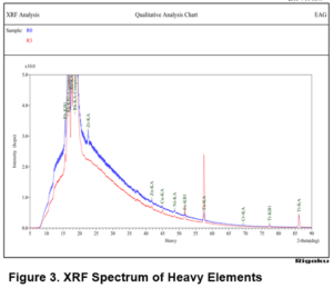
Recycled ABS Materials show numerous deleterious effects on molecular integrity of plastic materials, as seen in FTIR, XRF and GPC
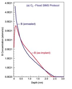
EAG’s PCOR-SIMS methodology includes point-to-point correction resulting in the most accurate SIMS profiling yet for ultra shallow implants.
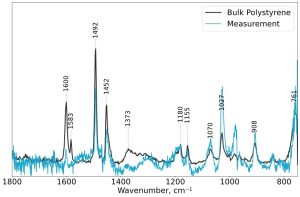
NanoIR is highly suited for identification of organic components that cannot be conventionally analyzed by other organic analysis techniques such as FTIR or Raman.
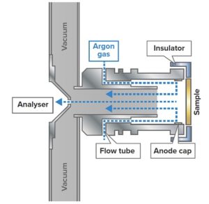
Ceramic matrix composites for aerospace materials must be of the highest purity. EAG presents FF-GDMS technique for robust chemical analysis.
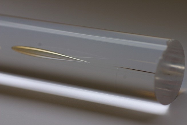
The chemical composition of all kinds of glass defects can be determined by SEM combined with EDS, XRF, Auger, and RGA.
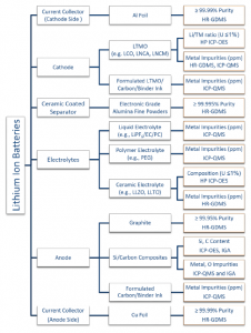
Chemical analysis techniques that can help to evaluate the composition of materials that are used for manufacturing Lithium Ion Batteries
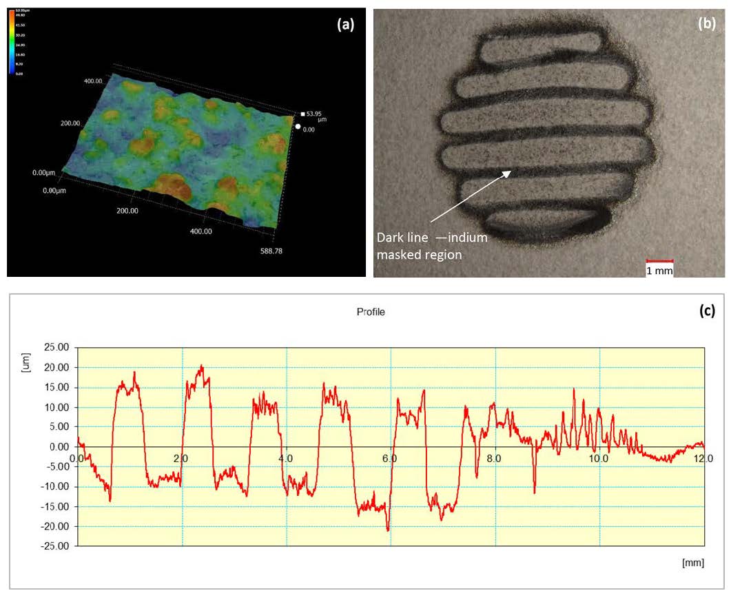
High resolution GDMS is recognized as one of the most versatile direct sampling techniques for survey chemical analysis of solids.
Biocompatibility testing of medical devices per ISO 10993-18 is a resource intensive process. Careful front-end study design leverages efficiencies to reduce timelines and minimize the total number of devices
required for testing.
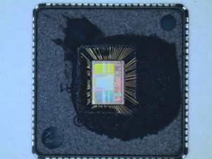
Chemical Decapsulation: Creation of a cavity on the package surface of an electronic component to expose the die underneath for inspection.
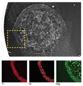
The chemical imaging of drug products helps to understand location/distribution of organic & inorganic constituents for formulation and IP

EAG evaluates chemicals & basic materials, helping to improve manufacturing, meet regulations, enhance research and resolve safety concerns.
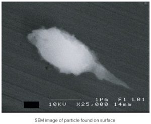
Airborne molecular contamination in cleanrooms lead to AMC defects in the electrical properties of wafers: Analysis by FTIR, GC/MS,TOF-SIMS .

EAG’s coatings testing lab provides deformulation, VOC EPA 24 testing, and other ASTM paint evaluations for product improvement and troubleshooting.
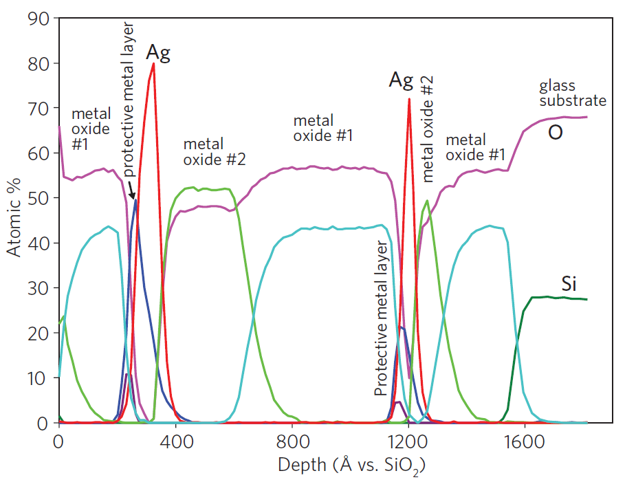
Investigation of the layer structure, identity and composition of an unknown coating system can be done in several ways.
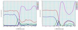
EDS and EELS are elemental analysis techniques integrated with electron microscopes such as TEM (Transmission Electron Microscope)
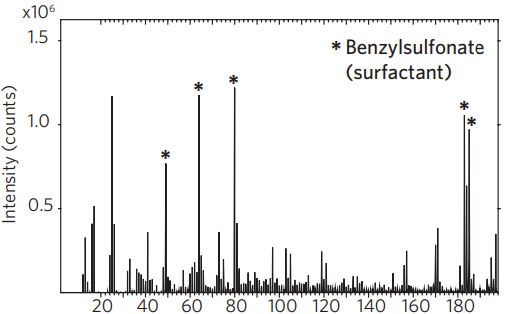
Glass development and glass product verification requires the measurement of composition with high accuracy.

Lithium-ion batteries (LIBs) are an essential technology for the clean energy transition currently in progress across the globe.
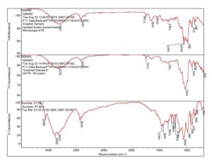
Contamination of great concern to the pharmaceutical and medical device industry, two case studies illustrate investigative approach.

EAG helps consumer products manufacturers build better by accelerating product innovation, improving raw materials & meeting all regulations.
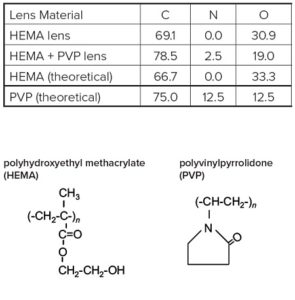
EAG Laboratories helps you understand contact lenses surface chemistry, critical to optimizing design and engineering optimal performance.

Medical device corrosion resistance optimized by using Auger depth profile & oxide layer thickness for device surface characterization.
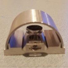
Cryogenic Focused Ion Beam (Cryo-FIB) uses traditional FIB techniques, but with a sample stage that can be controlled to -135°C.
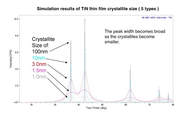
XRD analysis shows the crystallite size can be evaluated at half maximum of a diffraction peak as the crystallite size decreases.
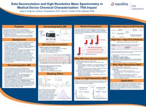
An accurate extractable profile from thoughtful Chemical Characterization translates to an accurate Toxicological Risk Assessment (TRA) and ensures patient safety.
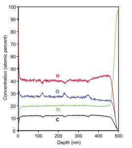
SIMS depth profile characterization provides accurate quantification for all measured species and matrix using our unique reference materials
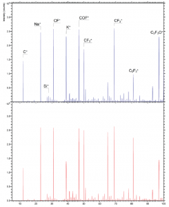
Cellphone screens are quite vulnerable to damage and are often protected with with a thin oleophobic coating.
Flame retardant materials determination – learn how our experts help understand this important product’s composition in this white paper
Thin films are widely used in many high-tech devices & consumer products. We discuss the processes used to measure the density of such films.
Dye and Pry is an excellent way to inspect a large number of bonds (leads, solder ball, seals..) at one time
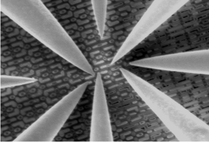
Nanoprobing is a highly specialized analytical technique used in semiconductor physics and electronics industries.
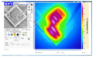
QFI Instrument Services and electrical localization services from EAG Laboratories are upgraded with LSM and XIVA image.
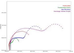
Electrochemical Impedance Spectroscopy (EIS) is a powerful, non-destructive diagnostic tool for monitoring the “vital signs” of lithium-ion batteries. Download the application note to learn more.

Electrolytes are minerals that carry an ionic charge when dissolved in solution. EAG can identify and quantify using Ion Chromatography (IC).
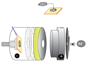
Photovoltaic Element Determinations by GDMS is ideally suited for trace element monitoring of PV grade CdTe/CdS materials.

Evaluating Surface and Oxide Composition of Electropolished Stainless Steel for High-Purity Gas Distribution Systems
Fine control over structural and compositional uniformity during epitaxial growth of compound semiconductors is critical for developing reliable and efficient devices.

The XPS surface analysis tool ensures evaluation of cleaning efficacy to monitor contamination efficiency.
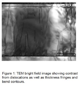
Threading dislocation evaluation of dislocation type in GaN using STEM (AN463) by EAG Laboratories supports LED development and quality.
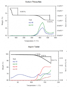
TGA with hyphenated technologies such as infrared (IR) and/or mass spectrometry (MS) is investigates the outgassing behavior of materials
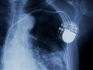
Exclusion Testing for Material Compliance Regulations of Medical Device Components has multiple regulating bodies.
Through database building, EAG provides higher-quality chemical characterization reports with reduced turnaround times to support medical device biocompatibility programs.
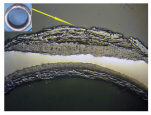
Failure analysis metals, nonmetals and composites for aircraft, aerospace, transportation, construction, consumer products, and electronics.

EAG Laboratories has the engineering expertise and advanced equipment and tools for microelectronic failure analysis of products and systems.
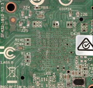
With in-depth images and analyses, EAG is able to examine the root cause of failures, critical dimensions, and quality of assembly process. Our experts can assist in PCB improvement.
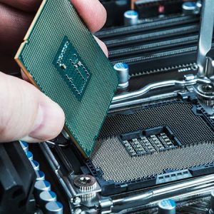
Failure inspection during post reliability stress testing to ensure no delamination, voids, cracks, material density changes.
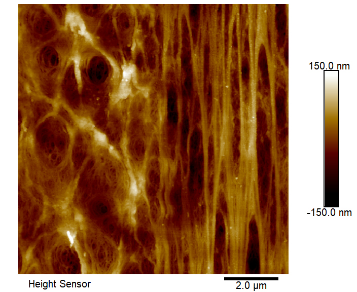
Atomic Force Microscopy (AFM) is used analytical technique for characterizing bio-membrane topography because it can be performed in fluid.
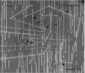
Focused Ion Beam (FIB) circuit edit techniques and FIB applications to help develop and improve IC design and advanced process nodes

Food testing services from EAG includes off-odors, off-taste, packaging interactions, extractables and leachables & materials identification

Food contaminant and beverage contaminant identification requires a strategic analytical approach using control and suspect sampling.

EAG experts guide manufacturers, processors and distributors through food investigations and help save time and money in crisis management.
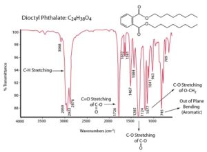
FTIR Services information from EAG Laboratories includes typical data, principles, strengths and limitations from our FTIR lab.
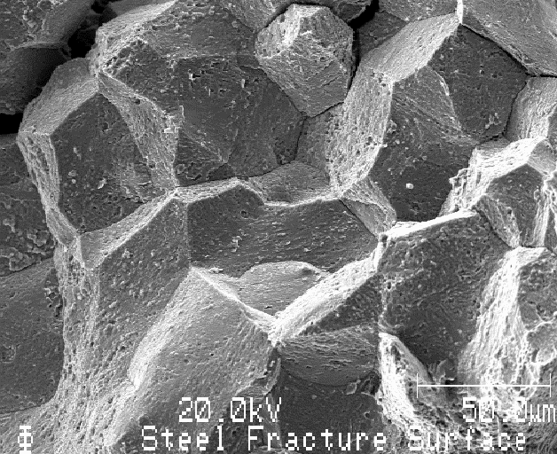
Characterization of metallurgical failures includes identifying segregation of elemental impurities to the surface of grain boundaries.
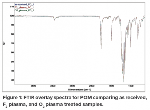
Fourier Transform Infrared Spectroscopy (FTIR) is a analytical technique for characterizing organic and some inorganic materials
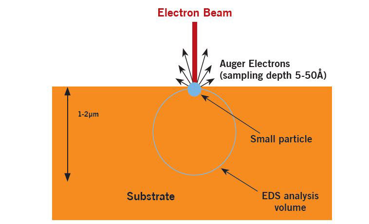
Auger (AES) spectra of small defects of various sizes shows excellent sensitivity is maintained down to a defect size of only 20nm.
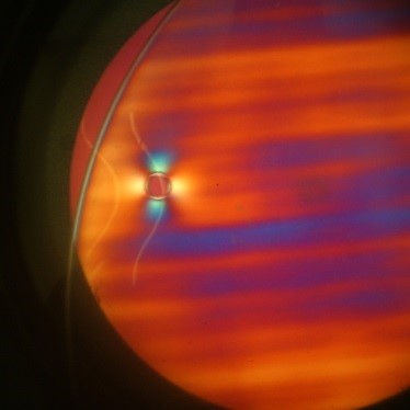
Glass faults or defects are inherent to the glass production process. In order to identify a defect, a range of techniques can be used
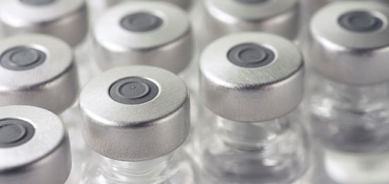
Application of SIMS, XPS/ESCA, SEM and ICP-MS to test for appearance of glass lamellae in parenteral pharmaceutical solutions, by EAG
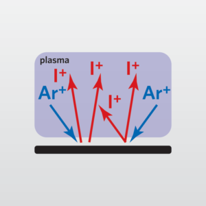
Glow discharge mass spectrometry (GDMS) is a robust analytical technique for direct determinations of elemental compositions of samples.
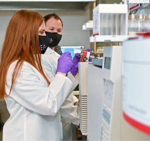
GLP characterization studies of test and reference materials by EAG Laboratories supports your regulatory compliance goals
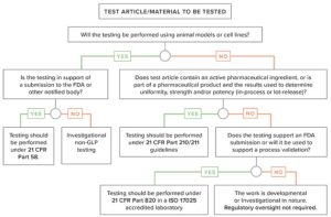
Medical device regulations are not entirely clear, EAG shows the decision process for contract analytical laboratories to support development.
Measurement of dopant & impurity concentrations in compound semiconductors by SIMS with low detection limits & excellent depth resolution.
HR-XRD Measurement of Compound Semiconductors can be used to determine the composition of strained layers and thickness.
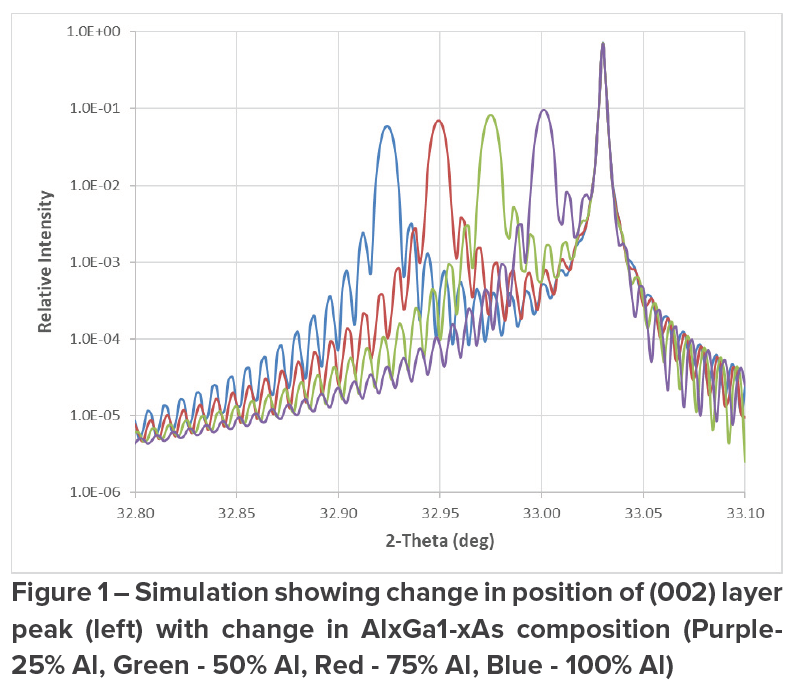
How to determine the composition of epitaxial thin films by X-ray diffraction and will focus on the analysis of AlxGa1-xAs thin films.
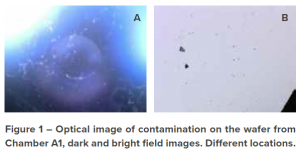
A concern with Stress testing of electronic devices is the potential contamination of devices by a poorly maintained or cleaned chamber.

EAG Laboratories has the skills and experience to analyze and troubleshoot every step of the aerospace flight process

Manufacturer-provided extractable data must be questioned and evaluated for your specific application. We outline the steps and questions.
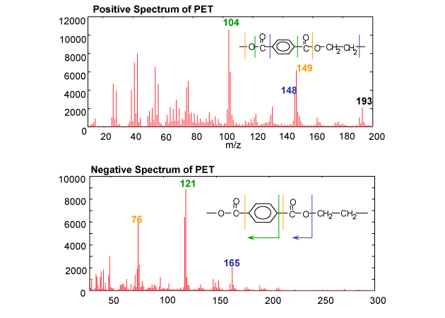
TOF-SIMS is a technique that can observe elemental, inorganic and molecular species present on the outermost surface of a sample
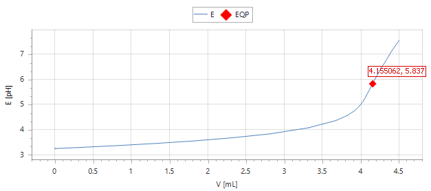
This application note highlights the importance of HF measurements in maintaining electrolyte quality.
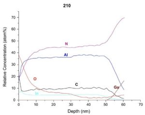
ALD for semiconductors can produce films that are high in H, C, O and metals. XPS and SIMS depth profile analysis for composition & purity.
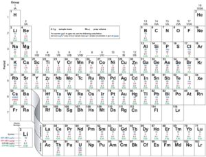
ICP-OES and ICP-MS detection limit guidance from EAG Laboratories is based on the strengths and limitations of these valuable techniques.
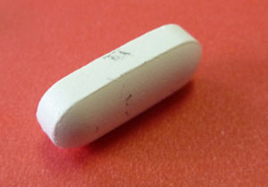
SEM-EDS and RAMAN analytical testing laboratory techniques applied to identification of foreign material contamination on pharmaceuticals.
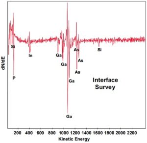
Auger Identification Interface Contamination is discussed regarding the elimination of contaminants for successful semiconductors.
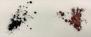
This paper describes identification of two unknown powders using Raman spectroscopy, combined with two X-ray techniques
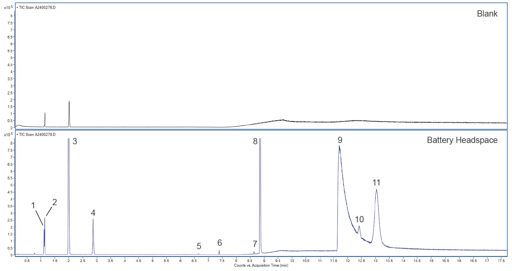
This application note describes the general screening approach of analyzing the gas within a swollen LIB pouch cell and identifying the chemical species present by headspace GC/MS.
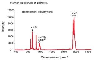
Learning the chemical composition of contaminants is challenging with small organic particles – Raman Spectroscopy is often the best approach
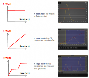
Additive manufacturing calls for powder feedstock of metals, alloys and ceramics, with particle size typically in 100s nm – 10s μm range.
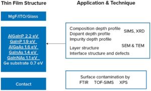
III-V solar cell technology for concentrator PV systems is the focus of this app note, illustrating the way that surface analysis can help
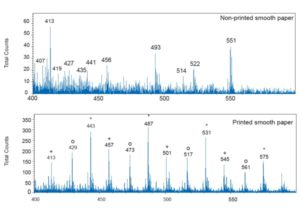
Imaging Cross-Sections by TOF-SIMS provides molecular information with high spatial resolution for the distribution of organic molecules
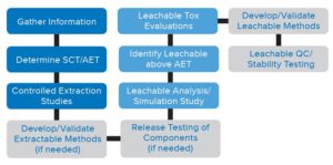
E&L methods pose challenges as they transition from R&D environment to routine QC testing. Understanding these challenges will help you avoid costly delays.
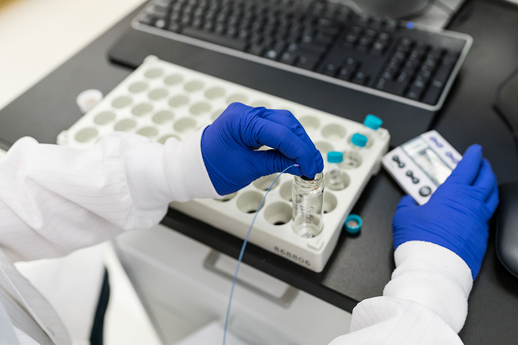
In chemical characterization studies, such as those performed for medical device biocompatibility testing under ISO 10993-18…
Battery characterization improves lithium-ion battery safety and performance using techniques such as SEM, TEM, XPS, GDMS, FTIR, ICP-OES, Raman and failure analysis
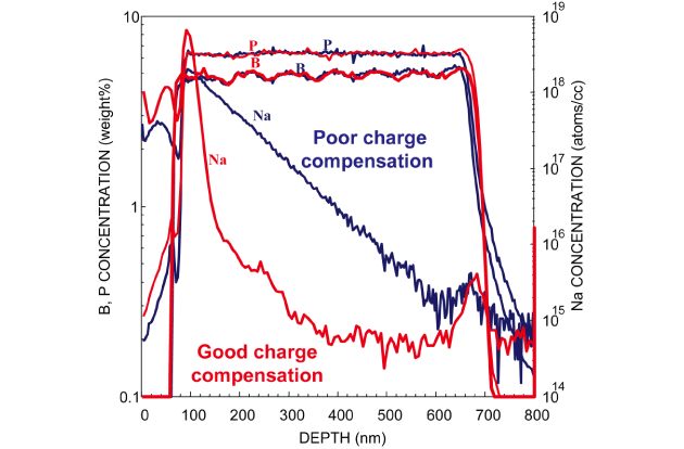
SIMS analysis is used to measure trace impurities in various materials such as semiconductors, metal, and insulating materials

EAG performs contaminant investigations and impurity identification across major dosage forms and delivery systems, such as unit dose vials.
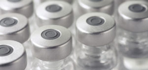
In Vitro Diagnostics test and system development support from the materials sciences experts at EAG Laboratories, contact us today!
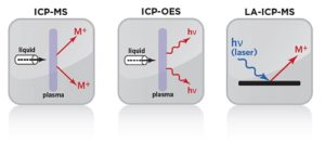
EAG offers comprehensive compositional analysis services, including “full scan” measurements of up to 69 elements, through its suite of Inductively Coupled Plasma (ICP) Analytical Techniques.
Industrial goods testing from EAG helps companies create innovative materials and troubleshoot problems with industrial chemical products.
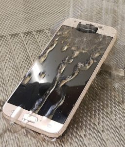
The type and degree of ingress protection that an enclosure possesses is described by the Ingress Protection (IP) rating.
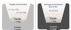
IGA Services from EAG Laboratories measures gas-forming elements (C, H, O, N and S) in samples from ppm to percentage levels.

The process of applying both PCOR-SIMSSM and STEM imaging to the same Si-SiGe multilayer sample demonstrates the individual strengths of both techniques and how they can be combined to form a complete understanding of the sample.
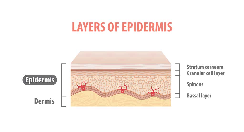
The data collected in this method validation indicates that the use of reconstructed human epidermal tissues provide an ethical alternative for assessing extracts collected from a product, including wearable technology and medical devices, for irritancy potential.

EAG is equipped with the necessary tools and techniques to examine hand sanitizer gel products for their primary ingredients
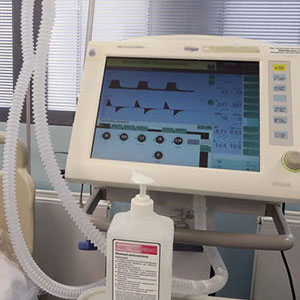
Respiratory protection testing, cleaning compatibility, sanitizing liquids and wipes, supply chain and manufacturing quality, failure analysis
LA-ICP-MS is an analytical technique that uses direct micro-scale sampling to provide high precision elemental and stable isotope analyses of solid maters
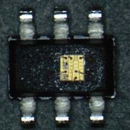
Laser decap at EAG Laboratories includes our Failure Analysis Laser Inspection Tool, view our picture book of PC boards before and after.

LED characterization, from process control to failure analysis to construction analysis, EAG Laboratories supports your LED analysis needs.
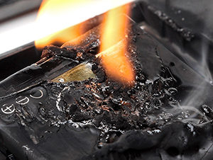
Level 1 Failure Analysis includes: non-destructive tests optical inspection, X-ray, C-SAM, and electrical characterization.
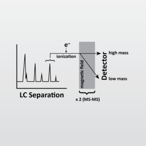
LC-MS-MS from EAG combines the separating power of liquid chromatography with the mass analysis of triple quadrupole mass spectrometry.
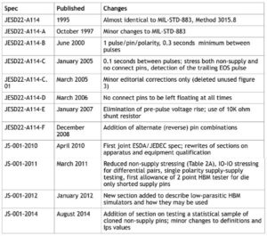
HBM ESD testing (Human Body Model electrostatic Discharge) uses the latest standards and best testing practices, reducing costs and time.

This App Note shows the approach of EAG Laboratories to test the material reliability of PLA Polymer Degradation
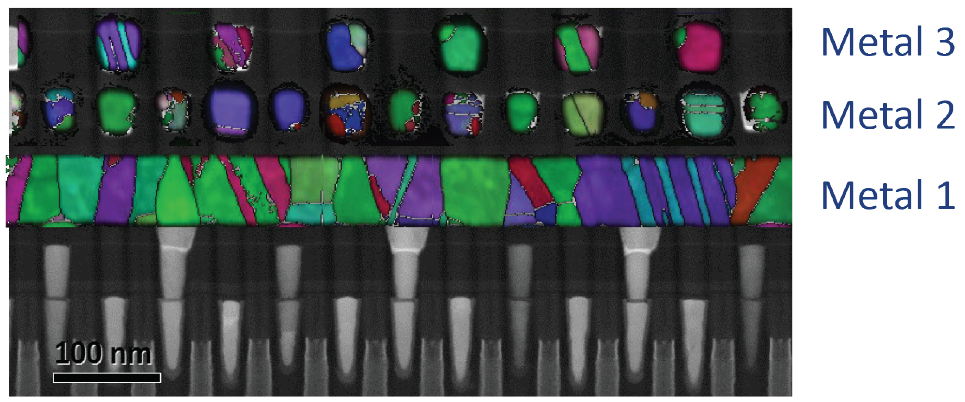
Examples of crystal grain orientation mapping and strain mapping in 7nm EUV technology IC chip and strained Silicon

Materials Characterization for Pharmaceuticals EAG has been contacted by pharmaceutical companies to characterize materials and chemistries where the measurements are challenging. We have developed methods
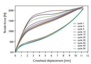
Mechanical testing incorporates the measurement of the material’s mechanical response to an applied force or displacement
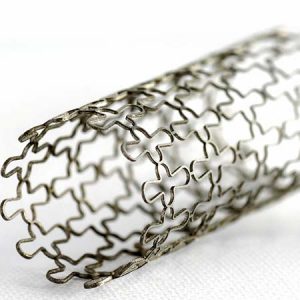
Drive productivity while keeping pace with evolving regulations
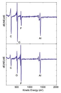
Auger Electron Spectroscopy applied to electronic circuitry problems involving the integrity of wire or ball bonding to metallic bond pads.

Device concept and medical device researchers need materials answers quickly so the can proceed with device development. Ask EAG!

Metallurgical testing lab services from EAG Laboratories includes grain size analysis, Rockwell hardness and image analysis.
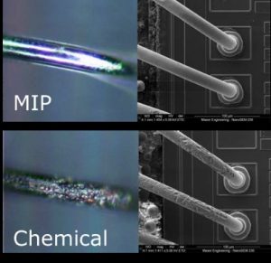
Microwave-Induced-Plasma (MIP) decapsulation allows for damage free removal of the protective cover of semiconductor packages.
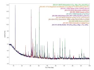
Microdiffraction can be used to identify crystalline inclusions in glass, look at film texture in a test pad on an integrated circuit, identify a single particle found in an air filter, or to identify the phosphor used in an LED.
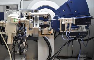
EAG has a new XRD/XRR instrument to help our clients solve challenging problems that require the analysis of small areas or volumes.

Mining materials analysis services include inorganic analysis, materials identification, failure analysis, and trace metal analysis
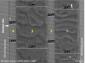
Understanding the construction/composition of films is beneficial for a variety of reasons
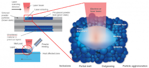
Additive manufacturing produces parts with geometric complexity, material composition gradient control, and lightweight structure design.
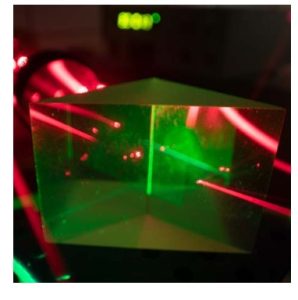
Glow discharge mass spectrometry (GDMS) relies on relative sensitivity factors (RSFs) in order to convert ion beam ratios of elements into mass fractions.
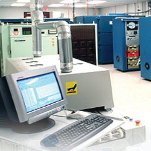
EAG has success executing burn-in programs for new product qualifications to conducting Early-Life Failure Rate studies.
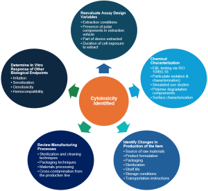
It can be alarming when a product with known components and extensive planning receives a cytotoxic result. Even if the sample was designed with materials marketed to be biocompatible, minor chemical reactions—from production of the raw materials to the packaging or storage of the product—can introduce cytotoxic contaminants.
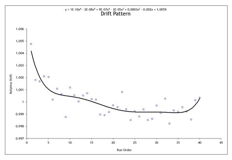
Complex oxides in energy storage, catalysis, sensor/actuation, optics, epitaxy substrates, electronics, bioceramics, structural ceramics
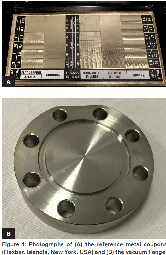
Characterizing surface topography is possible with a technique called Optical Profilometry (OP) also known as White Light Interferometry.
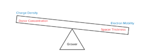
pHEMT device analysis by SIMS improves device performance and aids in failure analysis of III-V high-speed transistor structures.
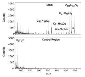
Time-of-Flight Secondary Ion Mass Spectrometry (TOF-SIMS) detects organic contamination on surfaces of semiconductors.

Orthopedic implants composed of metallurgical alloys, plastics and critical surface chemistries require characterization
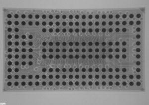
Package Delayering services helps to look for opens, shorts, leakage and damage in the layers and design rule distances in the sample.

EAG provides packaging analysis and innovation by combining analytical chemistry, polymer expertise and specialized microscopy techniques

Part 18: Chemical characterization of materials, part of ISO 10993 pertains to evaluating biocompatibility and safety of medical devices.
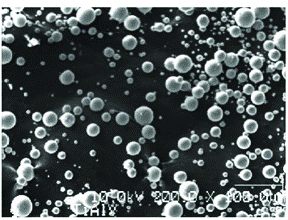
Particle analysis helps with black speck analysis, contamination identification, particulate analysis, identification of unknown materials.
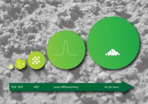
Particle size is an important parameter for many industrial processes
Point-by-Point Corrected SIMS (PCOR-SIMS) can determine accurate concentrations of matrix elements and dopants in GaN HEMTs.

Solving CSP qualification testing challenges by addressing key issues and applying specialized processes through EAG know-how.

EAG provides advanced testing to assist personal care and cosmetics brands, from deformulation to packaging studies to litigation support
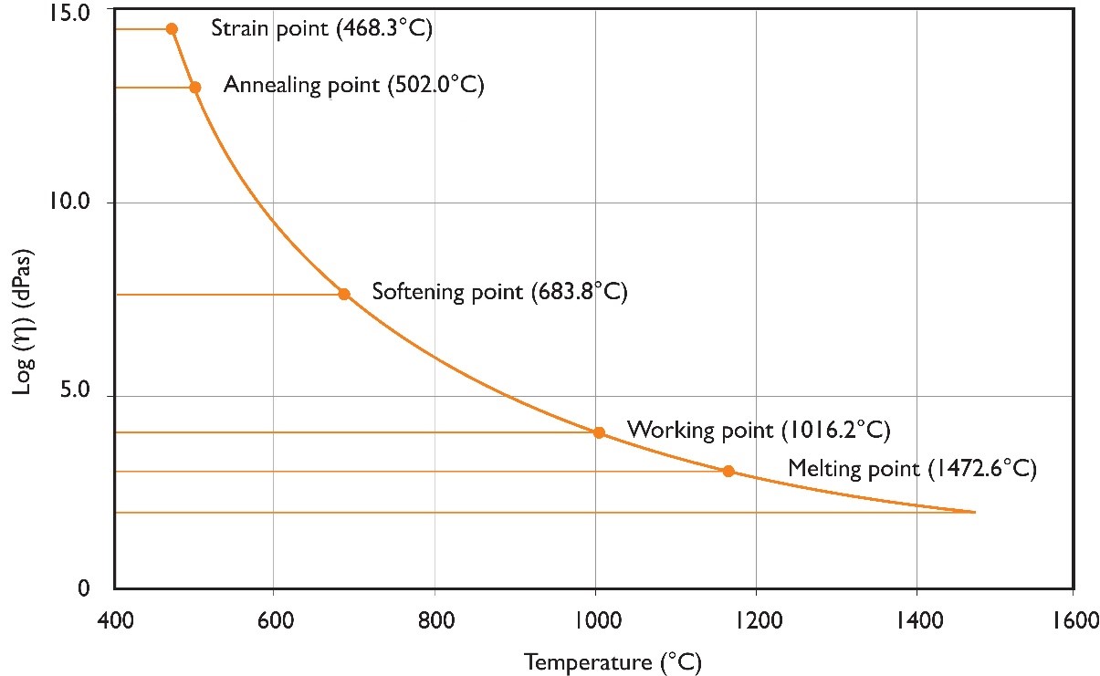
Viscosity is an important parameter for optimized glass processing, such as the viscosity temperature relationship of a glass.
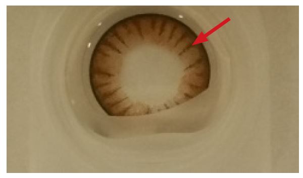
The contact lens market has expanded beyond its original goal of vision correction to include products with decorative qualities.
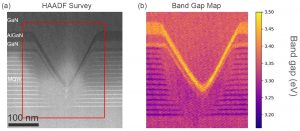
This application note highlights Eurofins EAG’s advanced monochromated EELS capabilities, including bandgap measurement, dielectric function extraction, plasmonic mode characterization, and high precision ELNES chemical state analysis.

Plastic deformulation studies help identify and quantify pigments, polymers, resins, impact modifiers, stabilizers and more in your products.
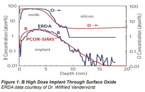
PCOR-SIMS is an EAG proprietary technique that can measure layer thickness, composition, and doping profiles.

Plastic testing services from EAG offers insight into thermoplastics, elastomers, thermosets, specialty polymers, polyurethanes, coatings.

EAG is excited to announce our latest sample preparation capability to address the emerging challenges of complex and advancing technologies.
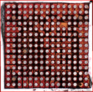
The common method of dye & pry can result in the cracking and shattering of die. EAG has altered the common dye & pry method, which has resulted in a significantly improved success rate.
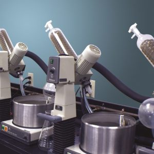
EAG offers product chemistry services: physical and chemical analyses to characterize active ingredients, product components and degradants.
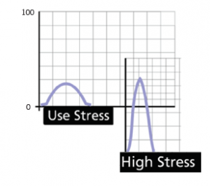
EAG has established product reliability test processes. In this example we inspect a Bluetooth speaker using Accelerated Testing.
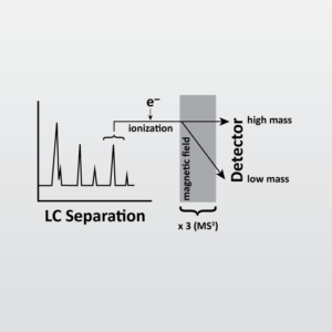
Quadropule Ion Trap (QTrap) The quadropule ion trap (QTrap) is a particular type of triple quadrupole mass spectrometer. Please refer to LC-MS-MS for a discussion
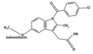
API Quantification on the Surface of Pharmaceuticals can be done by X-ray Photoelectron Spectroscopy (XPS) from EAG Laboratories.
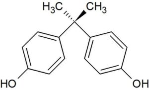
BPA analysis to quantify Bisphenol A levels in products using proprietary analytical methods using HPLC with a flourescence detector.
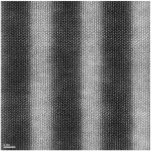
AC-STEM-EDS analysis is explored showing the effectiveness of this technique for characterizing ultrathin layers.
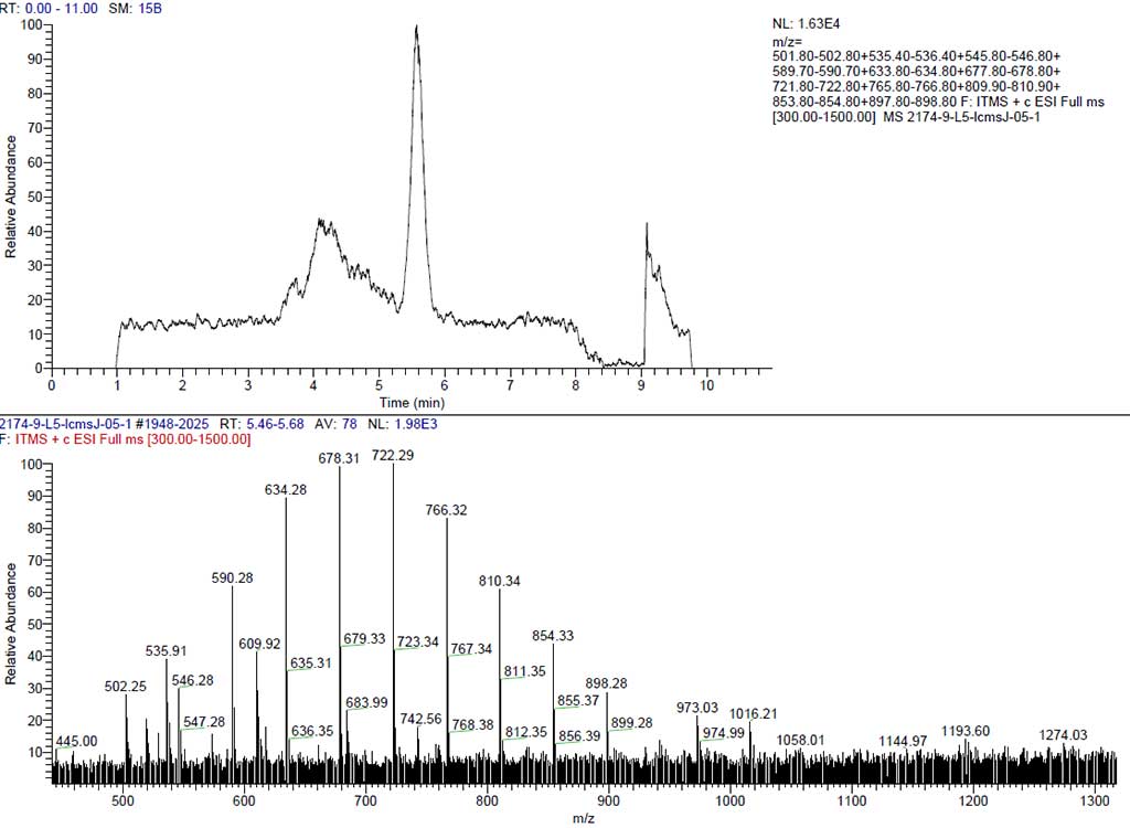
This method is for the quantitative determination of nonylphenols and nonylphenol ethoxylate (NPEs) by LC-MS.
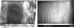
STEM provides images of dislocations with simplified contrast, allowing rapid dislocation typing in both cross section and plan view samples.
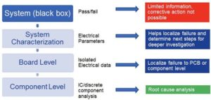
Electronic system failure analysis requires expertise in the modes of failures and techniques such as SEM, TEM, and dual-beam FIB.
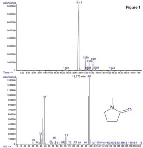
Detecting Levels of residual solvent concentrations in medical devices with Dynamic headspace Gas Chromatography-Mass Spectromety (GC-MS)
When information is required from a compound seminconductor, EAG can depackage and deprocess the sample, & fully characterize it.
Reverse engineering projects yield data regarding API & excipients for the development of generic formulations & resolving legal challenges.
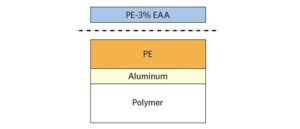
XPS and TOF-SIMS to solve adhesive failure of a polyethylene-ethylene acrylic acid (co-polymer) heat seal to polyethylene in a medical device.
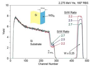
View typical RBS services results from EAG used for compositional thin film analysis for semiconductors, optimal coatings and more.
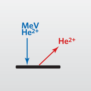
RBS Tutorial from EAG includes discussion of tandem accelerators, voltage sources, Kinematics, Scattering Cross Sections and Stopping Power.
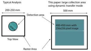
Impurities adversely affect performance of a CIGS solar cell, with varying concentrations – SIMS can help measure representative sampling.
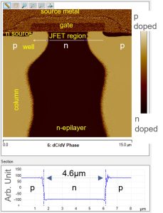
SCM provides doped region distribution mapping, profiling and dimensional analysis for the research and development, failure analysis and quality control of electronic components.
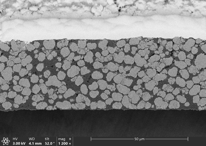
This application note outlines how SEM can be used to characterize battery electrodes, highlights key preparation methods, imaging techniques, and typical analysis goals.
SEM coupled with EDS provides high-resolution and high-depth-of-field images of
the sample surface along with elemental identification.
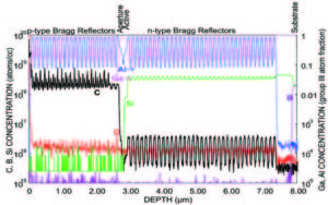
An advanced form of SIMS, PCOR-SIMS identifies dopants, impurities, compositions and thicknesses in various layers of VCSELs
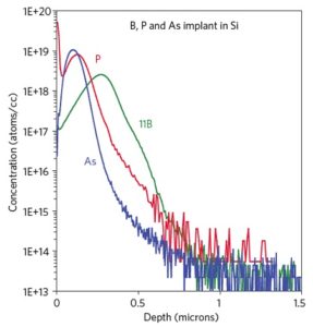
SIMS services from EAG is featured in this technique note, including sample data, showing how SIMS detects low concentrations of impurities
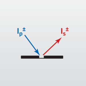
SIMS tutorial from EAG Laboratories includes SIMS primary ion sources, ion energy analyzers, Sputtering and elemental effects
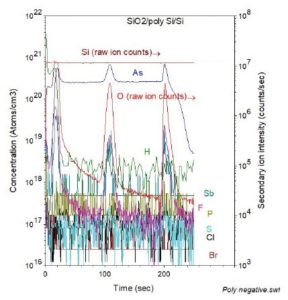
Survey-SIMS Depth Profiles analyze for dopants & impurities in a material without having prior knowledge in the structure being evaluated.
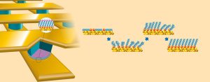
Self-Assembled Monolayers (SAMs) are used in molecular recognition, surface engineering, micro-contact printing and molecular electronics.
Semiconductor stress measurements by Raman Spectroscopy helps control problems related to stress control in semiconductor devices, from EAG.

EAG has support Aerospace and Defense customers for over 50 years

For over 40 years EAG has supported the Automotive Industry
Silicon wafer solar cells and the analytical techniques used to investigate failures, bulk defects and other materials characterization.
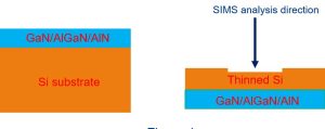
SIMS detects very low concentrations of dopants and impurities. It has been used to study the diffusion of Al and Ga.
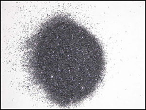
EAG’s SIMS Analysis Individual SiC Particles using a special sample preparation technique eliminates contributions from surface contamination
Raster change technique is used for SIMS measurement of very low levels of nitrogen in Silicon carbide by EAG Laboratories.
Secondary ion mass spectra measured by SIMS may not always provide information from the target element alone.
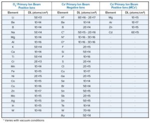
SIMS Detection Limits OF Selected Elements in GaAs, with detection levels are for normal depth profiling conditions of blanket wafers.
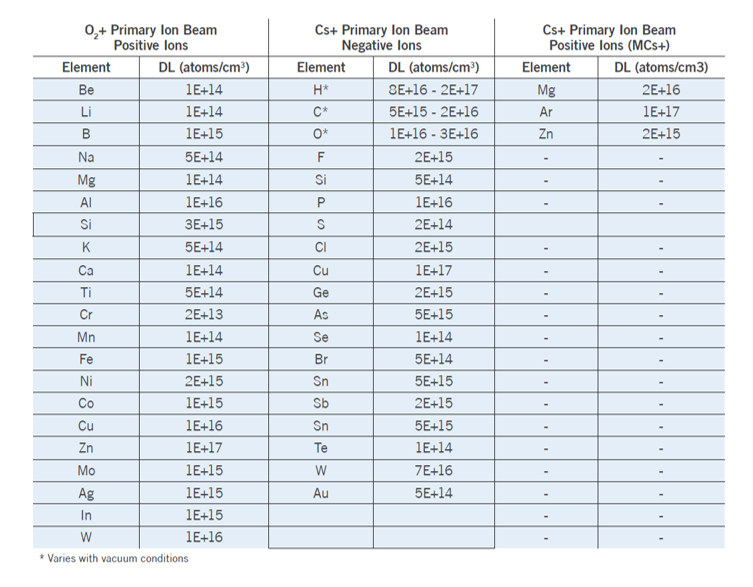
SIMS Detection Limits of Selected Elements in GaN. Normal depth profiling conditions, blanket wafers. Detection levels depends on area.
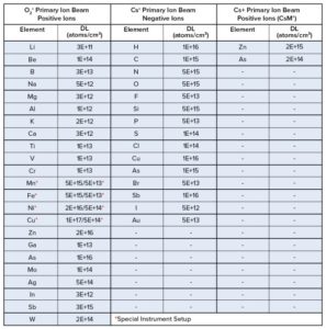
SIMS analytical technique typical detection limits for impurities in a HgCdTe matrix for normal depth profiling conditions.
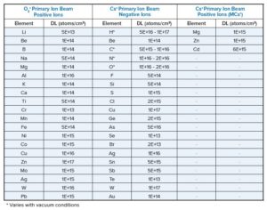
SIMS Detection Limits of Selected Elements in InP for impurities in InP matrices with normal depth profiling conditions.
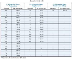
SIMS Detection Limits of Selected Elements in Si and SiO2 Under Normal Depth Profiling Conditions SIMS is a powerful analytical technique which allows detection of all
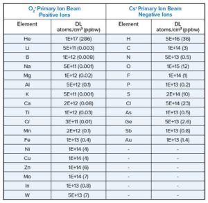
SIMS detection limits of selected elements in Silicon, providing a a list of detection limits for typical dopants and impurities
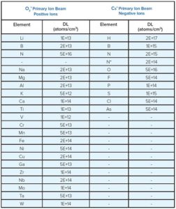
SIMS detection of all elements from H to U with excellent sensitivity. The table provides detection limits for impurities in a SiC matrix.
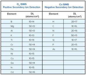
SIMS ZnO detection limits of selected elements under normal depth profiling conditions, showing overlay of SIMS profiles of arsenic implant
![SIMS measurement of Bulk [N], Table 1 Long term RSDs for three levels of [N]](https://www.eag.com/wp-content/uploads/2016/10/application-note-SIMS-measurement-of-bulk-N-in-nitrogen-doped-Cz-Si-long-term-precision-results-M-013716_Table_1a-300x150.jpg)
We have improved the SIMS measurement precision using the ASTM F 2139 test method and extended the detection capability into the 1×10¹³/cm3 levels.
Silicon Carbide SIMS Measurements provide valuable data for process control and problem solving in wafer growth and device manufacturing.

A paper on the early days of SIMS quantification and its evolution throughout the years.
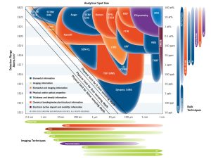
The EAG SMART Chart has graced the walls of leading labs and manufacturing companies for the past 25 years.

EAG provides solar industry with expert analysis of material properties, composition and chemistry to improve supply chain and manufacturing.
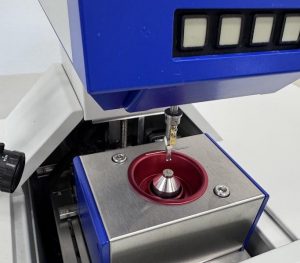
As electronic assemblies become more complex, ensuring high quality solder joints is critical for long term performance and reliability.
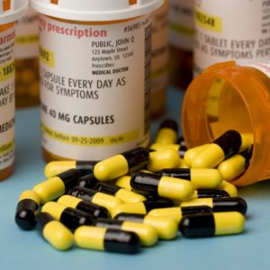
Specialized pharmaceutical services beyond a CRO support the convergence of new technology and pharmaceutical innovation.
Auger Electron Spectroscopy (AES) is effective in determining the quality of passivation layers to prevent corrosion in medical devices.
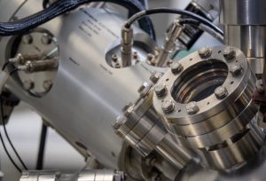
EAG Laboratories can offer a range of standards for SIMS used to calibrate materials such as Si, SiO2, SiN, Wsi, TiN, TiW, Al, GaAs, InP.
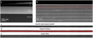
In this application note, we demonstrate our capability to generate a large number of measurements in a single image to determine the roughness of interfaces in a multilayer stack and the roughness correlation across layers.
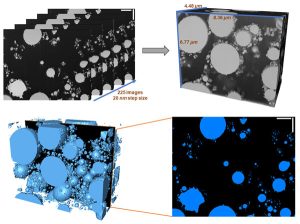
FIB-SEM tomography and image processing enable us to extract statistical analysis of particles from three-dimensional and high-resolution imaging data.
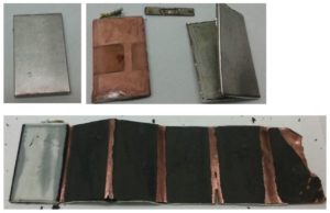
Structural and Chemical Characterization of Li-ion Batteries help to understand why batteries fail leading to safer products and improvements.
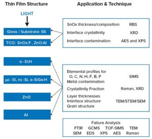
Surface analysis lab techniques on α-Si thin film PV, microcrystalline Si, nanocrystalline Si, amorphous SiGe, & microcrystalline SiC
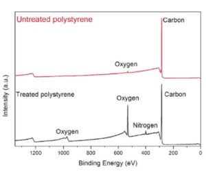
Analytical tools to understand chemical properties of polymers for adhesion, printability, barrier performance, appearance and strength
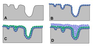
Surface area and pore structure are important considerations in many fields, impacting diverse industry concerns.
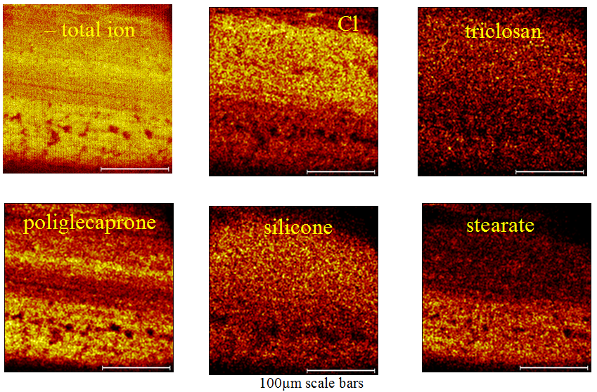
Antibacterial coated sutures reduce the occurrence of surgical site infections. Triclosan has been used in coatings on poliglecaprone.

Technology law covers the use of technology and covers all of the ways that devices and methods of communication impact society.

This application note presents a correlative approach combining scanning transmission electron microscopy (STEM) along with atom probe tomography (APT) to enable targeted, high-resolution characterization of MLCCs.

Analytical methodology to evaluate a variety of different face masks for a class of chemicals known as volatile organic compounds

Through multidisciplinary science and engineering, EAG helps companies translate ideas into technology by supporting R&D, NPI and production.

EAG Laboratories can test for ionic or covalent bonds at our Sunnyvale, St. Louis, Minneapolis and Eindhoven facilities

EAG offers analytical home and garden product lifecycle support, GLP registration and contaminant studies to label expansions and packaging.

RGA provides valuable data for optimizing battery safety, performance, and longevity.
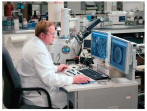
Paint deformulation separates out components to be identified with the normal analytical techniques available to the chemist.
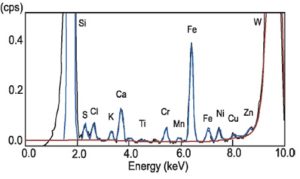
TXRF AND SURFACESIMS.XP is the total solution for surface contamination measurements on semiconductor surfaces, from EAG Laboratories.
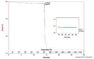
Thermal Analysis Techniques at EAG include TGA, DSC, TMA and DMA help with materials identifications, failure analysis and deformulation.
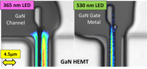
Eurofins EAG Laboratories has recently enhanced its thermal imaging capabilities with the integration of Microsanj equipment.
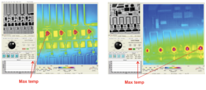
Temperature measurements of RF transistors to examine temperature distribution and look for areas of heating issues on many types of devices.
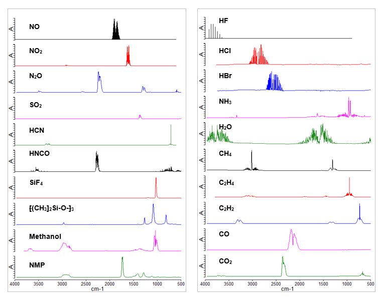
Synthetic polymers are widely used in many industry sectors. TGA-FTIR is used for materials characterization and outgassing profiling.
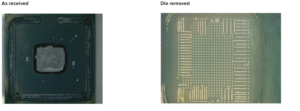
Time Domain Reflectometry (TDR) services from EAG – Each layer in the package may be inspected optically and probed electrically.

EAG has more than 20 years of experience in purity certification and trace elemental analysis of titanium and alloys following ASTM Test Methods.
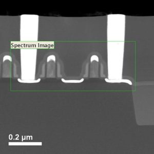
Two-dimensional mapping of matrix elements in electronic devices is discussed, as provided by STEM and EELS techniques from EAG Laboratories.

Transmission Electron Microscopy is often used to evaluate defects in crystals, but not all defects can be observed with TEM
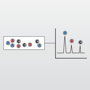
EAG uses ultra-high-performance liquid chromatography (UHPLC) to separate, identify & analyze different constituents of a chemical compound
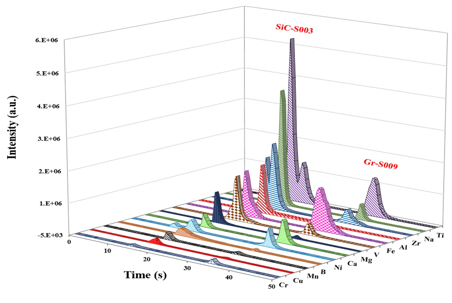
Electrothermal vaporization (ETV) coupled with ICP-OES is an exceptionally sensitive solid sampling technique for purity verifications.
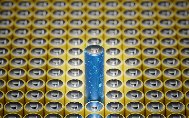
This application note introduces the principles of conductivity profiling using a platinum electrode probe and emphasizes its importance in battery electrolyte evaluation.
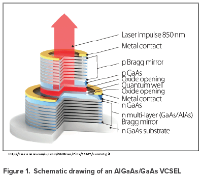
EAG Laboratories to provide comprehensive process development and failure analysis of vertical cavity surface emitting lasers.

Screen fruit juices for organic acids using high performance liquid chromatography with diode array detection.
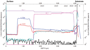
HEMTs characterization using SIMS helps to uncover troublesome impurities, optimize epitaxial layer growth and aid failure analysis
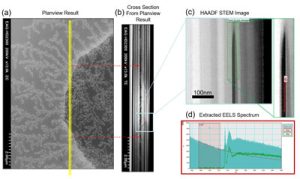
Improper aperture oxidation can lead to high stress or introduce unintended defects ultimately resulting in failure. Here, we present a study using STEM EELS to provide a method for measuring differences in oxygen bonding.
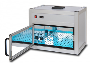
UV-C Irradiation For Product Reliability Testing Ultraviolet light (UV-C) is used for the disinfection of surfaces, air and water. It is able to destroy the

VOC testing of paints and coatings per EPA Method 24. EAG ensures your company meets standards for volatile organic compound testing.
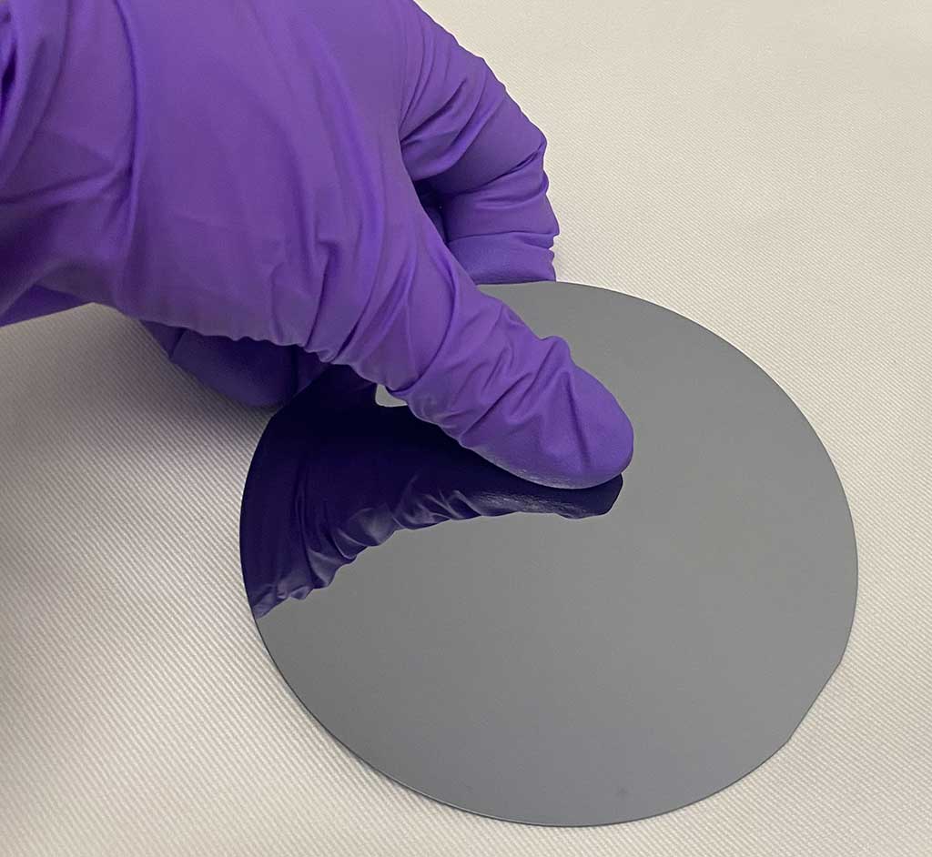
All disposable gloves tend to leave behind residues, which can affect the cleanliness of the surfaces the gloves touch, and thus possibly affect the analytical results.
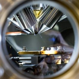
Comparing and summarizing the features of magnetic field type SIMS instruments and quadrupole type SIMS instruments
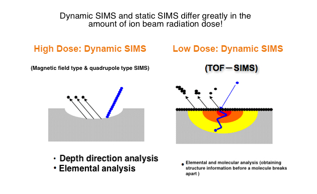
What is the difference between SIMS and TOF-SIMS? SIMS (Secondary Ion Mass Spectrometry) and TOF-SIMS (Time of Flight-SIMS) are the same in terms of mass
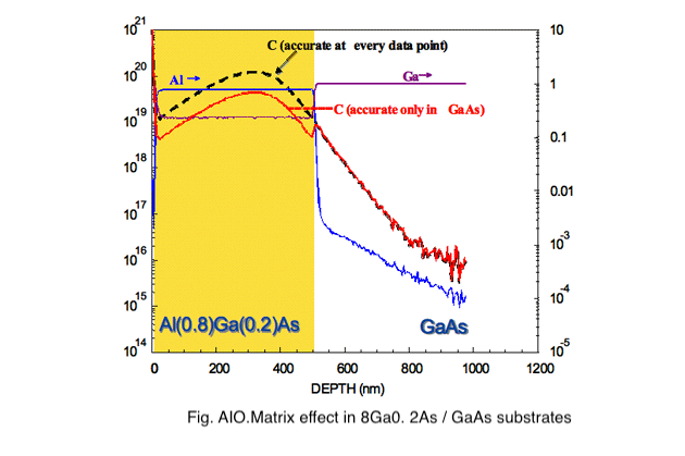
Compound semiconductor films are grown with different matrix compositions that affect the elemental sensitivities and sputtering rates
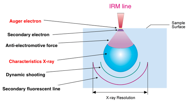
Both Auger Electron Spectroscopy (AES) and Energy Dispersive X-ray Spectroscopy (EDX / EDS) are used for elemental analysis.
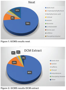
We employed a combination of GCMS, XRF and Fourier transform infrared (FTIR) spectroscopy to determine the composition of a Kombucha extract.
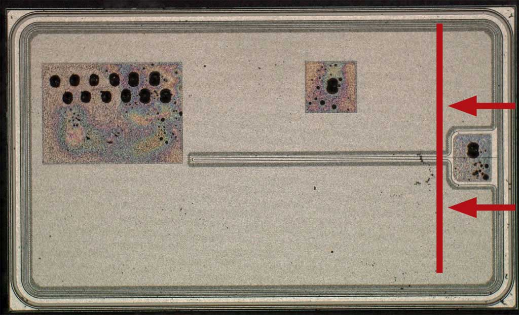
Cross sectioning of a semiconductor die is a basic step in failure analysis work. A cross section can be used as a check of layer integrity.
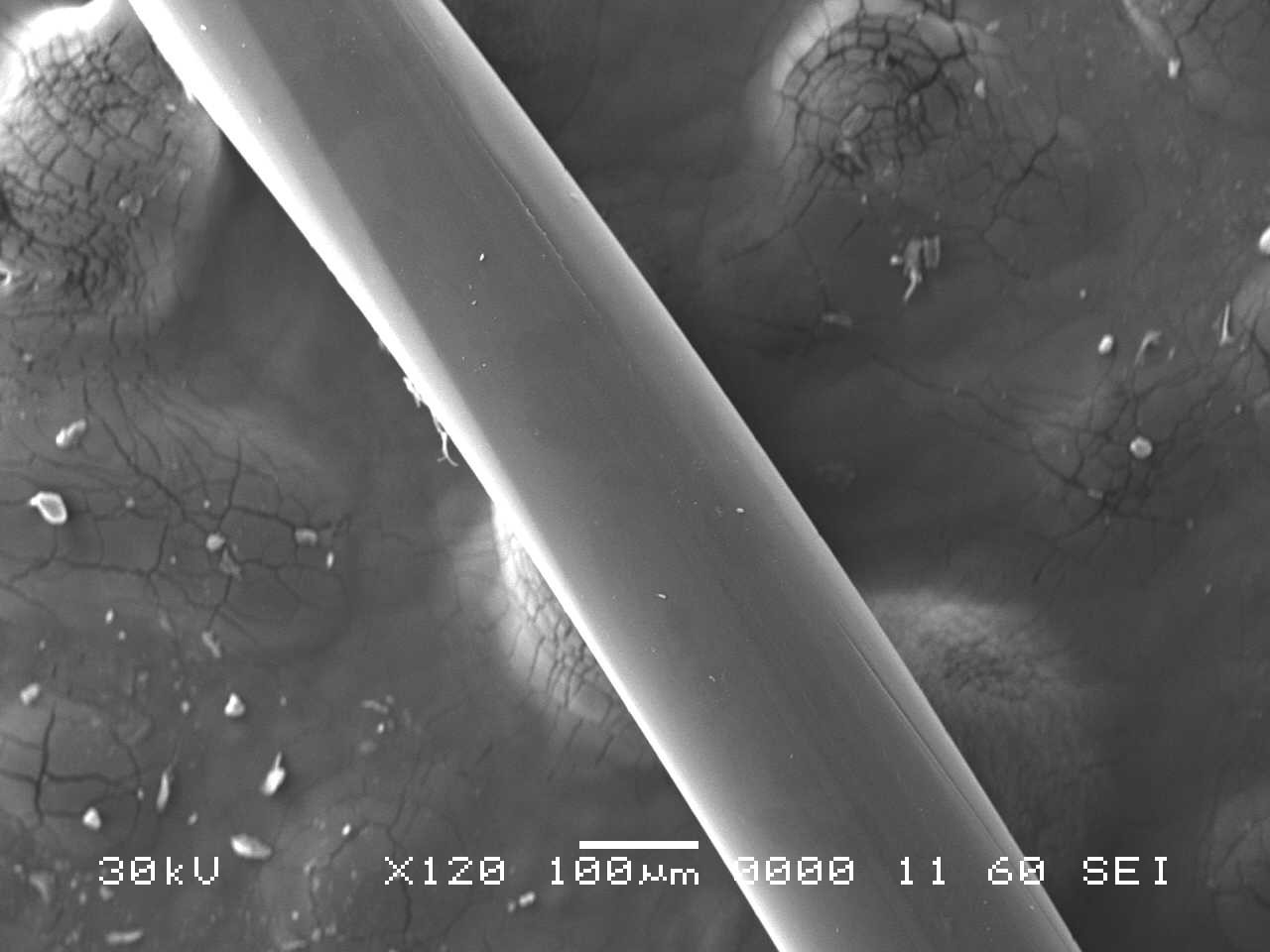
We investigate why Toothbrush bristles may begin to feel hard, stiff and rigid when compared to an unused toothbrush.
Consumer wearables are evaluated for sensitizers by extractable & leachable studies. We describe how to evaluate potential safety issues.
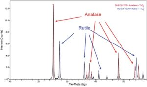
X-ray Diffraction XRD Services from EAG Laboratories is a powerful nondestructive technique for characterizing crystalline materials.
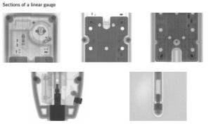
X-ray images from EAG include PCB layers, PC Board views, QFN, PCB Vias, QFP, Flip Chip, 9V Battery, BGA and BGA tilt and rotate.
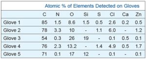
XPS Analysis of Disposable Gloves assesses materials exposed during product manufacturing to make sure contamination is not introduced.
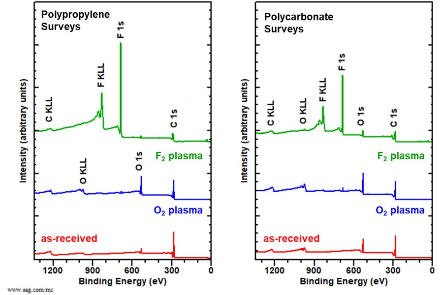
Polymer materials are in medical devices, automobiles, electronics, food packaging and in a wide range of industrial and consumer products.

XPS Analysis for sputter etching polymers and other organic materials to provide chemical characterization and depth profiling
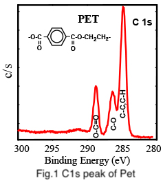
XPS (X-ray photoelectron spectroscopy) is capable of qualitative and quantitative analysis, and it can also determine chemical states.
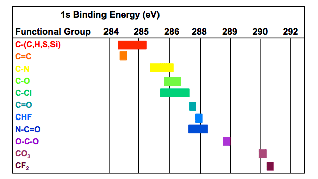
XPS shows the species present can be determined or estimated from the measured chemical shift of the binding energy of each element
To enable certain features and improve your experience with us, this site stores cookies on your computer. Please click Continue to provide your authorization and permanently remove this message.
To find out more, please see our privacy policy.