Silicon Wafer PV – Application Discussion
Home » Silicon Wafer PV – Application Discussion
Silicon wafer solar cells have been the mainstay of the PV industry, supplying about 90% of the PV worldwide. Cell efficiencies in the mid teens have been widespread and common, using fairly simple technology, and in the low twenties using more complex technologies at a few leading companies. As the PV Si feedstock shortage comes to an end and competition from thin film PV becomes more viable on a large scale, the Si solar cell technology challenge is to increase efficiency and reduce costs in order to achieve grid parity pricing.
The schematic of a common Si solar cell structure above illustrates some of the ways that surface analysis can help. Note that cell structures with efficiencies in the 20% range have key differences.
On the left middle side of the schematic we see a Si solar wafer that is 180 microns thick, or thinner. This substrate is doped with boron in the low 1016atoms/cm3 range if there is no compensation, and at higher levels if there is compensation. If the Si feedstock is upgraded metallurgical-grade Si and the process to make the Si wafer is a direct solidification design, there will be high levels of nitrogen, carbon and oxygen in the substrate, and most likely high levels of metals.
The top side of the wafer (the side which receives the light) is textured. The actual texturing structure varies, especially for multi-crystalline substrates, but also for single crystal substrates. Phosphorus is added to the textured surface, and a silicon nitride is deposited as an anti-reflective coating (ARC).
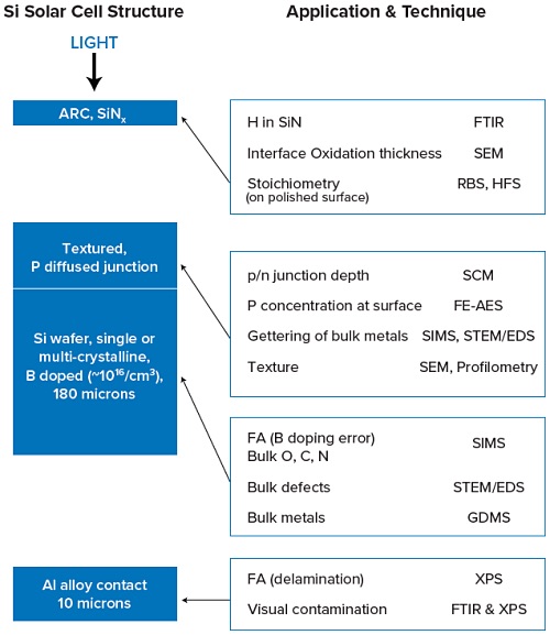
Metal contacts are added to the front side and the backside. Thermal processing is used to diffuse the phosphorus into the boron-doped substrate, form the ohmic contacts on the front and back, and getter metal impurities away from being recombination centers. In principle the phosphorus diffuses conformally into the textured silicon surface, and hydrogen from the SiN diffuses into the substrate to passivate defects. Optimization of the thermal process for all these effects is one of the main engineering challenges.
On the right side of the schematic we see that failure analysis of the lower metal contact can be supported by XPS, and FTIR. For the silicon wafer, doping errors can be determined by SIMS. Bulk total concentrations of [O], [C], and [N] can be measured by SIMS; FTIR does not provide total concentrations. Bulk defects can be analyzed by STEM/EDS, and bulk metal surveys can be done by GDMS.
For the upper layer of the silicon wafer, P concentrations at the top of the textured Si can be determined by FE-Auger, the p/n junction depth may be determined by cross section SCM (Scanning Capacitance Microscopy). The latter is under development at EAG. The texture itself, which in some cases can be quite complex and unexpected, can be characterized by profilometry or cross section SEM for finer spatial resolution. Gettering of metals can be analyzed by SIMS or STEM/EDS.
The ARC can be analyzed for H by FTIR. If there is an oxide layer between the ARC and textured Si, cross section SEM may be able to measure the thickness, and cross section STEM/EELS can verify the presence of O in the layer. If the ARC layer is deposited on a flat Si sample (not textured), RBS and HFS can provide stoichiometry
Would you like to learn more about testing of Silicon Wafer PV?
Contact us today for your silicon wafer PV testing needs. Please complete the form below to have an EAG expert contact you