Precession Electron Diffraction (PED)
Home » Our Techniques » Imaging » Precession Electron Diffraction (PED)
PED analysis provides visualization of material phase, crystal structure and strain level at nanometer (nm) scale. Typical applications of PED include phase mapping, crystal grain orientation mapping, grain size distribution analysis, texture analysis, grain boundary analysis on poly-crystalline materials, and strain level mapping on single crystalline materials.
PED analysis is a great complement to other structural analysis techniques, such as Scanning Electron Microscopy (SEM) based Electron Backscatter Diffraction (EBSD) and X-Ray Diffraction (XRD). Performed in Transmission Electron Microscopy (TEM) setting, PED offers visualization of structural information at higher resolution, but often requires more complex sample preparation. Eurofins EAG is the only service lab to offer PED analysis services to all users.
Ideal Uses of PED
- Structural analysis for poly-crystalline materials, such as semiconductor metal line, via deposition, metal/ceramic film, poly-Si film:
- Visualization of materials nanostructure through phase mapping and crystal grain orientation mapping
- Crystal grain size distribution and average grain size analysis
- Preferential growth direction characterization/ texture information through pole figures
- Strain level mapping for single crystal, such as strained Si/SiGe, III-V materials quantum well devices
Strengths
- Can provide visualization of materials structure at nm scale
- High strain detection sensitivity (< 10^-3 level)
Limitations
- Significant sample preparation and analysis time (several hours to days)
- Relatively small sampling volumes (<5X5um)
- Plan-view characterization can be challenging
- Materials with complex crystal structure, e.g. some ceramics, can be challenging
- Requires prior knowledge of materials phase/structure, which can be determined by other techniques, e.g. EDS, EELS, XRD, etc.
Precession Electron Diffraction Technical Specifications
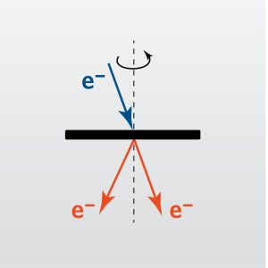
- Signals Detected: Diffracted electrons
- Elements Detected: All elements, assuming they are present in crystal form
- Detection Limits: Grain size > 5nm
- Depth Resolution: No Depth information
- Imaging/Mapping: Phase mapping, Crystal grain orientation mapping, Strain level mapping
- Lateral Resolution/Probe Size: ~ 2nm
Would you like to learn more about using Precession Electron Diffraction (PED)?
Contact us today for your Precession Electron Diffraction (PED) needs. Please complete the form below to have an EAG expert contact you.