Material structural analysis power of PED at nanometer scale
Home » Material structural analysis power of PED at nanometer scale
As the new technologies continue to progress in recent years, materials characterization for such devices and processes becomes ever more challenging. Materials characterization, including chemical/elemental analysis and structural analysis, needs to be performed not only at higher sensitivity but also at much smaller scale.
For structural analysis, traditional XRD and SEM based EBSD has been providing materials structural information with great precision. However, until recently, the emerging TEM based Precession Electron Diffraction (PED) technique has started bringing this analysis to the nanometer scale, which has been essential to meet the demand of the nano-scale structural analysis at the nowadays aggressively size-shrinking technologies and processes.
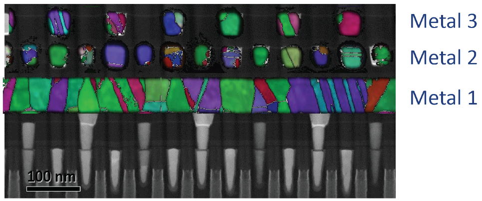
In this application note, examples of crystal grain orientation mapping and strain mapping in various devices (7nm EUV technology IC chip and strained Si) are shown to exemplify the material structural analysis power of PED technique at nanometer scale.
Would you like to learn more about material structural analysis?
Contact us today for your material structural analysis needs. Please complete the form below to have an EAG expert contact you.