In the world of technology, innovation and continuous improvement are imperatives—and being able to quickly and reliably test, debug, diagnose failures and take corrective action can make the difference between a doomed product launch and building a successful global brand.
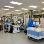
EAG Engineering Sciences offers you the world’s largest and most diverse collection of specialized analytical instrumentation, capacity to perform a variety of microelectronic tests in parallel, and the multi-disciplinary expertise required to critically evaluate results and provide true insight into a solution.
Learn More About EAG's Engineering Sciences Services
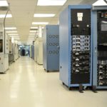
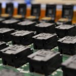
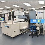
Our wide range of ATE test equipment and experienced team can support first silicon debug thru release to high volume production for a wide array of products, ranging from Digital to RF, including wafer sort and packaged part testing. Our 24/7 production floor can support complex test flows and end product fulfilment, and many customers find they can support their entire production volume needs in EAG’s secure test environment.
Our burn-in and reliability qualification lab is one of the finest in the country, with over 75 chambers and ovens, tight ESD safety controls, routine audits, and a dedicated engineering staff to provide you with all of the burn-in, package qualification, process qualification, and other reliability data you need.
DPA (Destructive Physical Analysis) is performed on “high reliability” electronic components and materials used in aerospace, commercial, military and government applications.
EAG Laboratories is an industry leader in ESD testing (Electrostatic Discharge) and latch-up testing. Our highly experienced engineering team uses their industry leading knowledge and years of real world experience with the latest semiconductor technologies, circuit design and device physics to optimize our customer’s ESD and latch-up results.
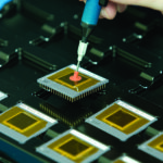
EAG’s failure analysis team comprises a highly technical and professional group of engineers with a wide range of backgrounds and experiences from diverse industries including semiconductor, medical device, aerospace, military, automotive, laser, solar and manufacturing.
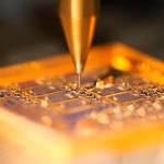
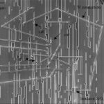
Focused Ion Beam, or FIB circuit edit, services allow the customer to cut traces or add metal connections within a chip. Our services include sample preparation, sample analysis, fault isolation, circuit modifications and a full range of debug tools.
Our PCB team offers a wide variety of standard-style reliability testing hardware solutions, as well as ESD and ATE interconnect solutions for multiple and large pin count device testing, with fair pricing for the quality and integrity of all your test hardware.
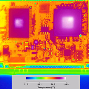
Warpage Analysis allows for measurement of warpage and deformation of products that are subjected to thermal stresses. This analysis produces a 3D topographical profile.
Whether you need to develop and execute a robust test plan, debug early prototypes, determine the root cause of a failure quickly or ramp up production of your product, EAG Laboratories can help. We offer you the world’s largest and most diverse collection of specialized analytical instrumentation, capacity to perform a variety of microelectronic tests in parallel, and the multi-disciplinary expertise required to critically evaluate results and provide true insight into a solution.
Would you like to learn more about Microelectronics Test & Engineering?
Contact us today for your Microelectronics Test & Engineering needs. Please complete the form below to have an EAG expert contact you.
To enable certain features and improve your experience with us, this site stores cookies on your computer.
Please click Continue to provide your authorization and permanently remove this message.