Microwave Induced Plasma Decapsulation (MIP)
Home » Microwave Induced Plasma decapsulation
Microwave-Induced-Plasma (MIP) decapsulation allows for damage free removal of the protective cover of semiconductor packages, including 3D, SiP, WLCSP, High Tg, Chip on Board, and BOAC. Microwave Induced Decapsulation has many advantages compared to traditional wet-etch decapsulation. For example, when a device contains Cu and Ag based bond wires they can be damaged from the traditional chemical etchants.
Microwave Induced Plasma decapsulation (MIP) vs RIE Plasma etching
Typically, EAG uses a 13.56 MHz Reactive Ion Etching (RIE) Oxygen plasma systems to decapsulate which reduces the damage caused by chemical etching. In most situations this method of decapsulation works well.
Microwave Induced Plasma is an option when there is a need to further reduce the risk of any damage to the device. A Microwave Induced Plasma decapsulation system is capable of a much higher etching rate than RF plasma systems where longer RIE etches can cause the sample to heat up. Microwave-Induced-Plasma uses O2 radicals that are generated in the 2.45 GHz plasma that are efficient in etching the epoxy in the molding compound and the ultrasonic cleaning process is efficient in removing the silica fillers.
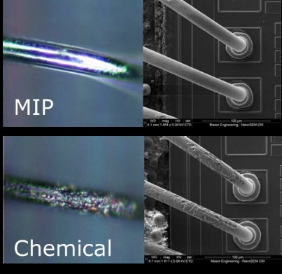
Microwave Induced Plasma decapsulation is able to decapsulate epoxy molding compound effectively with no damage to the bonding wires encapsulated therein and the aluminum bond pads on the semiconductor die. This is due to the microwave ions having a short travel life in any direction, which reduces the potential of damages compared with a RIE plasma etch system caused by ion bombardment and electrical stress.
Decapsulation of a device is the first start of the Failure Analysis process. EAG’s failure analysis support starts with engineer-to-engineer interaction to discuss and comprehensively understand your issue, challenges, goals and urgency. EAG engineers are knowledgeable and experienced in today’s advanced technologies and products and are experts in failure analysis.
One Stop Shop
EAG has more than 30 years experience supporting companies in the total product lifecycle from conception thru volume production. An example is our testing services which offer 24/7 production, pilot, prototype test and the capability to rent our tools for onsite program.
EAG Engineering Sciences offers you the world’s largest and most diverse collection of specialized analytical instrumentation, capacity to perform a variety of microelectronic tests in parallel, and the multi-disciplinary expertise required to critically evaluate results and provide true insight into a solution.
Would you like to learn more about Microwave Induced Plasma decapsulation (MIP)?
Contact us today for your Microwave Induced Plasma decapsulation (MIP) needs. Please complete the form below to have an EAG expert contact you.