Advanced Surface Analysis for Problem-Solving in Flat Panel Display Manufacturing
Home » Advanced Surface Analysis for Problem-Solving in Flat Panel Display Manufacturing
The manufacture of modern flat panel displays involves the use of advanced high technology processes and materials. Production of TFT-LCDs (Thin film transistor liquid crystal displays) involves the merging of traditional Si semiconductor processing technology with glass processing and fine chemicals.
This application note focuses on the use of TOF-SIMS (Time-of-Flight Secondary Ion Mass Spectrometry) for the analysis of residue formed during a TFT manufacturing step. TOF-SIMS provides highly specific chemical information (both atomic and molecular) from the top 10-30Å of a surface.
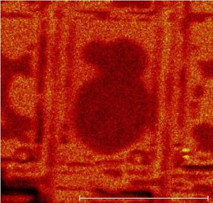
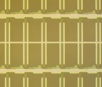
In this case, circular defects filling almost whole cells were found to be present during inspection of the display. A typical area of the TFT structure is shown on page 2. Each cell is about 100µm wide. The defects were only visible when liquid crystals were present within the structure and the defect positions were noted at that point. The defects were suspected to be organic in nature.
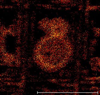
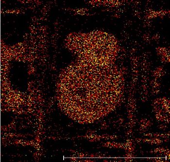
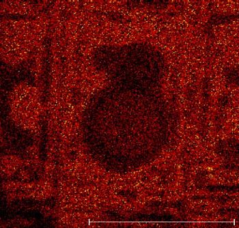
TOF-SIMS data can be displayed as either ion images or as mass spectra. The images below show the lateral distribution of selected species on a TFT surface. Mass spectra show the specific molecular and atomic species present in a particular region within the image, in this case, from the defect.
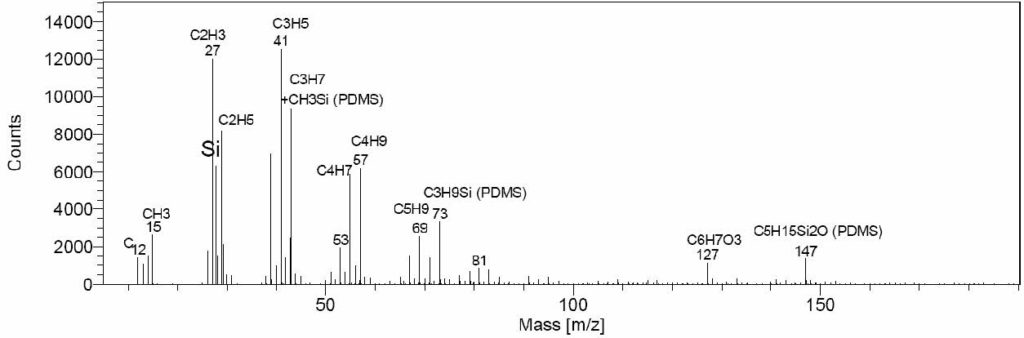
Shown here are the total ion image (all positive ions from the sample), and also positive ion images for Si, C3H9Si and C2H3. The defect is the dark circular area in the middle of the total ion image. The Si and C3H9Si map with the defect whereas other organic ions (e.g. C2H3) do not. C3H9Si and other ions marked in the mass spectrum are due to PDMS (polydimethylsiloxane). PDMS is widely used in industrial materials, as a polish, mold release agent, lubricant, pump oil and also as a component in some adhesives. Page 2 shows a positive ion mass spectrum obtained from the defect. In this failure analysis example, the PDMS was traced to a specific source within the manufacturing process. This example illustrates the important and useful information that can be obtained using the correct analytical instrumentation to address a manufacturing problem in the FPD industry.
m/z 28, Si
m/z 73, C3H9Si
m/z 27, C2H3
Optical image of analytical area of interest
Positive Ion TOF-SIMS Spectrum of a Defect on a Flat Panel Display
Would you like to learn more about Advanced Surface Analysis?
Contact us today for your flat panel display manufacturing analysis needs. Please complete the form below to have an EAG expert contact you.
To enable certain features and improve your experience with us, this site stores cookies on your computer.
Please click Continue to provide your authorization and permanently remove this message.