Cleanroom Materials as Sources of Airborne Molecular Contamination
Home » Cleanroom Materials as Sources of Airborne Molecular Contamination
Every material introduced into a cleanroom is a potential source of Airborne Molecular Contamination (AMC). The chemical composition of a material, its surface area, its thermal behavior and the temperature ultimately determine the levels of contamination introduced into the cleanroom environment by a specific component. Those contaminants that condense on critical process components can lead to “AMC defects” such as changes in the electrical properties of wafers, uncontrolled boron and phosphorus doping, etch rate shifts, threshold voltage shifts, wafer and stepper optic hazing and high contact resistance. As line widths of microelectronic devices shrink “AMC defects” have become a major concern and need to be considered in the design of cleanrooms.
The condensable Airborne Molecular Contamination arising from various cleanroom materials has been studied by means of FTIR, GC/MS and TOF-SIMS. In addition, the transfer of contaminants by direct contact was also investigated. The latter is of interest since contact transfer may result in the spread of contaminants over a large area of the cleanroom. In both experiments silicon wafers were used as substrate material.
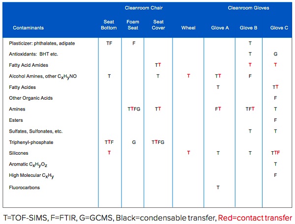
Table 1 summarizes the results for different parts of a cleanroom chair and from 3 different cleanroom gloves. The letter indicates the technique by which a contaminant was detected, the color of the letter indicates whether a contaminant was detected as condensable AMC (black) or by contact transfer on a wafer (red).
Due to its high sensitivity for most condensable AMCs, TOF-SIMS detects a significantly larger number of contaminants than GC/MS or FTIR. TOF-SIMS also allows for detection of contaminants transferred by direct contact. The ability to identify specific contaminants with high sensitivity is of critical importance to meet requirements for contamination control and for an optimized selection of cleanroom materials.
The analytical methods discussed here can also be used to investigate incidences of cleanroom contamination due to chemical spillage and to monitor subsequent cleanup efforts.
Would you like to learn more about Cleanroom Sources of Contamination?
Contact us today for your Airborne Molecular Contamination needs. Please complete the form below to have an EAG expert contact you.