With STEM-EELS, each point in the image can be directly linked to a spot in the elemental distribution maps. The technique has excellent lateral resolution (~1nm) that allows mapping of non-planar features in the target device.
DISCUSSION
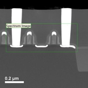
A High Angle Annular Dark Field (HAADF)-STEM image of a Si-based MOSFET device is shown in cross-section in Fig. 1. In this imaging mode the contrast is dependent on the average atomic number of the material.
Within the imaged area, there are three transistor gates with alternating source/drain contacts made of NiSi and two TiN-lined W contacts. A 2-d STEM-EELS map was acquired with a selected pixel resolution of 5nm × 5nm and signals for Si, Ni, N, O & Ti were monitored.
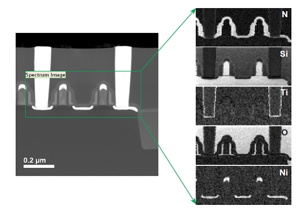
Figure 1 HAADF-STEM Image showing the region outlined in a green frame from which a 2-d STEM-EELS spectrum map was acquired.
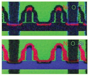
Figure 2 Composite RGB distribution maps for Ni (red), O (green) and Ti (blue) above and N (red), O (green) and Si (blue) below.
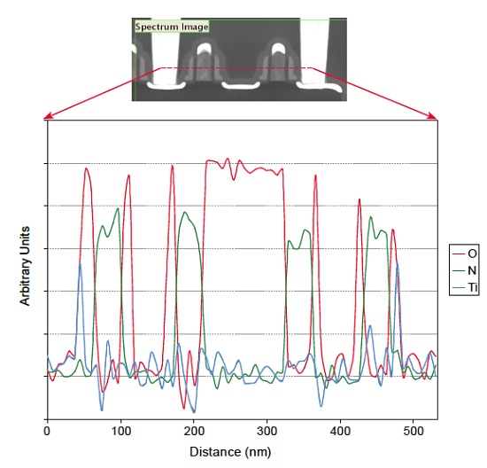
The signals are mapped as composite images in Fig. 2 and as individual distribution maps in Fig. 3. From the raw 2-d EELS spectrum image data set it is possible to extract a line-profile in any orientation. One such example is shown in Fig. 4.
However, it should be noted that, for the present case the signals for O, N and Ti are noisier than if a separate EELS acquisition was optimized for just these three elements. This is a tradeoff between mapping elements spanning a large energy loss range and the exponential fall in EELS signal intensity with increasing energy loss.
In the present case a wide energy loss range was monitored to include signals from Si (L2,3 @ 99.2eV) to Ni (L2,3 @ 854eV) with the core loss edges of Ni, Ti and O occurring in between (@ 401.6eV, 455.5eV & 532eV respectively).
Figure 3 Individual elemental distribution maps for N, Si, Ti, O and Ni are shown above.
Figure 4 HAADF-STEM image with location of extracted line profile superimposed on it (red dotted line). Elemental distribution profiles along that line are plotted below the image. It is possible to extract similar line profiles from any orientation and length within the green frame.
Would you like to learn more about Mapping of Elements in a Microelectronic Device?
Contact us today for your elements in a microelectronic device by STEM-EELS. Please complete the form below to have an EAG expert contact you.
To enable certain features and improve your experience with us, this site stores cookies on your computer.
Please click Continue to provide your authorization and permanently remove this message.