Performing Reliability Qualification Testing On CSP Without Damaging Devices
Home » Performing Reliability Qualification Testing On CSP Without Damaging Devices
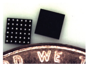
System miniaturization, especially in the handset market, is driving the development of advanced packaging technologies to accommodate products as thin as 6 millimeters (mm), or less. Unfortunately, traditional epoxy plastic packages are simply inadequate for building these extremely thin smartphones and other mobile devices, as their footprint area is up to 6 times bigger than the chips they house.
The solution of choice for cellphones and other handheld and wearable electronic products is Chip Scale Packages (CSPs), which are the same size as the chips, themselves. CSPs are attached directly to circuit boards using solder balls. Unfortunately, the size advantages that make CSPs so attractive also make them fragile and susceptible to damage during handling. This has created a need for new ways to qualify devices so that failures are understood, screened before they invalidate reliability qualification, and not introduced during the very process intended to screen for them.

THIN IS “IN,” MOVING INDUSTRY TO MORE FRAGILE PACKAGING
Today, the state of the art for smartphones is 7.6mm thick for the iPhone 5, which compares to the earlier iPhone 4S and iPhone 4 at 8.8mm and 9.5 mm thick, respectively. Since batteries and screens aren’t shrinking, the size of the packaging and substrate board must be reduced in order to achieve these thin product profiles, which has driven the move to CSPs.
Packages are getting smaller, so the qualification challenge is getting larger. According to Brandon Prior of the research firm Prismark, the 5S was the first mobile device to use 50 µm line/space (L/S) and CSPs on a 0.4mm pitch. Prismark forecasts that more than 28 percent of CSPs and wafer-level CSPs (WLCSPs) will be at 0.4mm or less by 2018.
Qualcomm’s senior director of package engineering, Steve Bezuk, discussed packaging challenges at the IMAPs Device Packaging Conference in March 2014, saying that, while very few packages during the late 2000s were WLP, this category now accounts for nearly half of IC packages.
Meanwhile, CSP substrates are getting even thinner. The SEMI global industry association serving the manufacturing supply chain says that today’s leading-edge CSP substrates have 15 micron (µm) lines and spaces, and are moving toward even finer lines and spaces so they can handle fine bump pitch of ≤110 µm. In its report titled “Global Semiconductor Packaging Materials Outlook – 2013-2014,” SEMI said that substrate vendors are targeting 5µm lines and spaces, as well as 40µm via diameters in the build-up layers in 2015. The report said that core layers are being fabricated with 12µm lines and spaces, with vias as small as 50µm and capture pads as small as 110µm.
These and related trends continue to make CSPs increasingly difficult to handle, and even more prone to damage prior to and during the qualification process. In general, the CSP reliability qualification process must address four key issues: handling; incoming and outgoing quality control (IQC/OQC); socketing; and unbiased stress testing.
Handling – The raw and very brittle exposed silicon material in a CSP can easily suffer stress cracking during handling. This can create imperfections in the silicon matrix, which can cause the resulting cracks to propagate with the additional stress of various qualification processes. These and other dynamics make it extremely difficult, for instance, to differentiate between CSP failures induced by qualification-related stress tests, and those induced earlier during handling. The problem becomes even more challenging at the high volumes of consumer smartphones and other mobile devices, and with the growing premium on thin product profiles.
IQC/OQC – This process is difficult and costly to automate, and therefore must be performed through visual inspection by technicians with proper training. Metrics are often an issue, requiring customized specifications in order to optimize screening effectiveness for the given device.
Unbiased Stress Testing – Unbiased stress tests include preconditioning moisture sensitivity, reflow, high temperature storage (HTS), temperature cycle tests (TMCL) and highly accelerated stress test (uHAST). These tests are relatively straightforward for non-CSPs because they’re larger with more mass, and less fragile. If the same procedures are used with CSPs, though, this will generally lead to device damage. Solving the problem requires choosing solutions for protecting the CSP during these unbiased stress testing, including using carriers and other custom fixtures, and providing training in how to use them.
Socketing During Stress Testing – Parts must not only pass unbiased stress tests, but also biased tests including biased stress testing and bias reliability qualification testing, in which the part is powered up and exercised. Biased tests can include high temperature operating life (HTOL), high temperature cycle, early failure rate (EFR), and burn-in. During biased tests, a part generally goes into a socket, and the socket makes the electrical connection to the board, as an alternative to soldering parts to a board for these tests. This requires the use of sockets or, in some cases, specially designed daughtercards. Tests might range from high temperature operating life tests, to biased versions of other tests. This ensures that parts can more easily be removed after testing; however, it can still be challenging to get the parts in and out of their sockets without damaging them.
SOLVING THE PROBLEM
The solution to these challenges is to apply a combination of a) specialized processes, b) carriers and other custom fixtures as an alternative to sockets and daughtercards, when needed, and c) operator training covering all aspects of the qualification process.
Specialized Processes – Most important is to implement 100% top and bottom visual inspection, in order to screen out damaged parts before stress testing is initiated. EAG has collaborated with several customers on customized top and bottom inspection specifications that focus on how to measure dimensions to optimize screening effectiveness. Any missed devices will invalidate the entire lot, so the key is screening parts before putting them into stress, so that a valid sample quantity is used.
Selection of Sockets, Daughtercards and Custom Fixtures – For biased stress testing, it is important to make the proper choice between sockets and, increasingly, a specially designed daughtercard, which requires experience in designing burn-in and HTOL/HAST boards with both socket and daughtercard approaches. For unbiased stress testing where the part does not need to be powered, custom fixtures called carriers are often required.
EAG has experimented with a variety of carrier materials and structures for protecting CSPs during stress tests, including small baskets with covers or a “top hat” that covers the device so it isn’t bumped, blown around or otherwise impacted and damaged. Material is important for protecting the CSP because the carrier is also exposed to extreme environmental conditions.
An additional challenge is to create a carrier that is large enough so that the CSP isn’t damaged when being inserted into and removed yet not so large that it can move around inside and become cracked. Each carrier can hold up to 240 parts and is unique to the device and custom-designed for the correct size of the CSP.
Operator Training – Training is required on issues including how to properly perform inspection, the types of defects to look for, and how to handle parts (if needed) to minimize damage. If sockets will be used during biased stress testing, training is also required on how to insert CSPs into sockets and safely remove them.
Training will also be required on the use of custom fixtures if they are implemented. Any staff involved with the CSP qualification process will need to be trained, and the most valuable training is generally on the job. EAG has gone through considerable trial and error in order to derive best practices that apply to most scenarios, including developing the most effective screening processes, carriers and other elements.
BEST PRACTICES IN CSP QUALIFICATION
EAG has helped customers with CSP qualification for quite some time and, as a result, has established a number of best practices. While no two challenges are precisely alike, there are recurring issues that must be resolved.
For instance, a major chip supplier for mobile devices was having an issue with a high level of damage during stress testing. Qualification lots were being invalidated at an unknown point in the multi-step process, requiring the customer to start all over again. The resulting delays were particularly problematic because of the pressure to hit milestones in an industry with extremely sensitive launch cycles.
Analysis showed that the problem originated upstream at an assembly house where the devices were being diced and bumped. The devices were exhibiting cracks from improper handling of the parts. The solution was to institute an inspection process for outgoing devices at the assembly house, including 100% top and bottom visual inspection. EAG initiated this visual inspection process, which revealed the source of the problem at the assembly house. EAG then trained operators at the customer site on the types of things to look for, and provided guidelines for ongoing inspection. After instituting these steps, the customer is now able to screen out 100 percent of damaged parts before stress tests begin. Solving this type of problem is increasingly important because of the dynamics of today’s multi-tiered semiconductor supply chain.
In another example, a customer that manufactures ICs for consumer electronics devices was having problems with CSP cracking and chipping from the effects of airflow equipment during unbiased stress tests. Although the airflow was very minor, it was causing approximately 20 percent of the tested parts to be damaged as they were moved around, invalidating the entire screening lot. EAG designed a patented, custom fixture that allowed devices to be secured properly, eliminating the problem at its source.
CONCLUSION
Resolving CSP qualification challenges requires experience with a number of complex issues across a wide variety of customers and situations. Best practices require the use of specialized processes, the proper choice of sockets, daughtercards or customized fixtures (including specialized carriers for biased test socket insertion), and highly trained equipment operators and inspection technicians. With the right implementation, there should be less than 8 percent “fallout” on a good lot, ensuring that no lots will be invalidated at any point upstream or downstream in the complex CSP qualification process.
Would you like to learn more about Reliability Testing On Chip Scale Packages?
Contact us today for your reliability qualification testing on Chip Scale Packages. Please complete the form below to have an EAG expert contact you.