Statistical Analysis of Multilayer Structures in Electron Microscopy Using Image Processing
Home » Statistical Analysis of Multilayer Structures in Electron Microscopy Using Image Processing
Image processing can be used to generate high density critical dimension measurements that allow us to extract the full profile of the interfacial roughness in a multilayer stack.
Electron microscopy images play a critical role in semiconductor device characterization, allowing engineers to visually inspect devices and measure critical dimensions relevant to their performance. This process of measuring critical dimensions can be repetitive and time consuming when done manually. Although this is less of an issue when only a few measurements are needed, these issues can become prohibitive when it is necessary to examine the full profile of a specific dimension across the entire image or when measurements need to be made across many images. In these cases, automatic image processing is required to extract the critical dimension information. In this application note, we demonstrate our capability to generate a large number of measurements in a single image to determine the roughness of interfaces in a multilayer stack and the roughness correlation across layers.
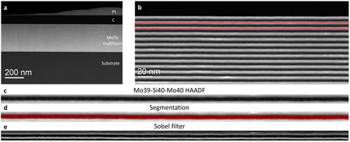
(a) HAADF STEM image of a Mo/Si multilayer stack. (b, c) Higher magnification views of the top layers from a. The highlighted layer in b is the Si layer chosen for analysis and shown in a cropped view in c. (d) The segmentation of the Si layer in red is based on an intensity threshold. (e) The resulting image after a Sobel filter is applied.
Would you like to learn more about STEM?
Contact us today for your STEM needs. Please complete the form below to have an EAG expert contact you.