High Depth Resolution SIMS Profiles for Compound Semiconductor Devices
Home » High Depth Resolution SIMS Profiles for Compound Semiconductor Devices
The measurement of dopant and impurity concentrations with depth in compound semiconductors is often accomplished using Secondary Ion Mass Spectrometry (SIMS) because of its very low detection limits and excellent depth resolution. SIMS is a key analytical technique for research, development, and process control of compound semiconductor epitaxy and devices.
One of the challenges for SIMS is to continuously improve its excellent depth resolution capability to meet some of the increasing demands of compound semiconductor structures. SIMS depth resolution, or the ability to distinguish real impurity or matrix concentration differences with depth into the sample, is affected by many physical parameters. These include the topography of the sample, the mass of the primary ion, the impact energy of the primary ion beam striking the surface, the shape of the primary ion beam (i.e., lateral ion intensity distribution), and the instrumental ability to separate secondary ions originating from the center of the SIMS crater versus those from the crater sidewalls.
Conditions required to achieve desired detection limits may also affect depth resolution. The SIMS depth resolution capability is a complex compilation of factors that must be optimized for each application.
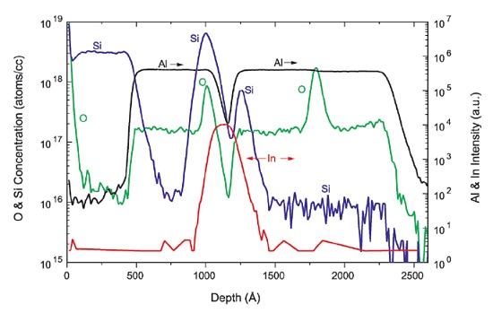
Some examples that illustrate advancement in SIMS depth resolution capability, and value to the semiconductor engineer, are given here for HEMT structures. Figure 1 is a SIMS profile of Si, O, In and Al in an AlGaAs/InGaAs HEMT structure. The primary ion is Cs+ and the impact energy of the primary ion is 2 keV. The combination of a heavy primary ion (Cs) and a low impact energy (2 keV) is necessary for optimum depth resolution.
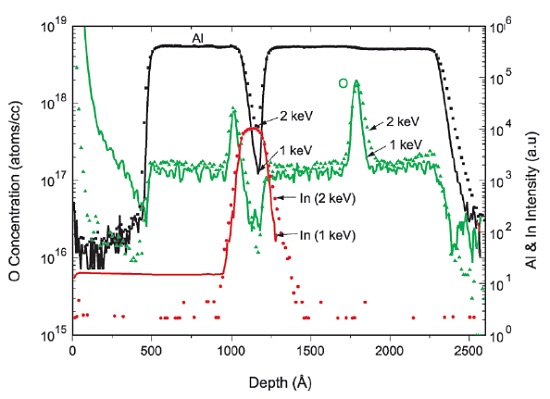
The same sample was analyzed using a 1 keV impact energy, so that a comparison could be made between depth resolutions derived from 1 keV and 2 keV impact energies. Figure 2 is an overlay plot of the Al, O and In signals for 1 keV (solid lines) and 2 keV (dotted lines). First consider the Al signals. At about 1100Å nm the Al signal drops sharply at the first interface of the InGaAs layer. The sharpness of this drop is greater for the 1 keV impact energy and the apparent “valley” of the Al signal is deeper for the 1 keV impact energy. This is a direct result of improved depth resolution. For the In signal we see a similar effect in that the sharpness of the In decrease at the second interface (~1300Å nm) is greater for a 1 keV impact energy. For the O signal we see the width of the interfacial oxygen concentration at about 1750Å nm is more narrow for a 1 keV impact energy, and the sharpness of the falloff of oxygen signal is greater for a 1 keV impact energy.
Figure 2 Comparison of O and Al profiles at 2keV and 1keV
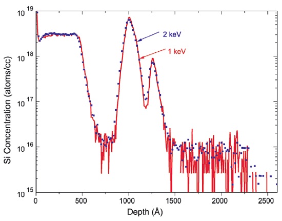
Figure 3 Comparison of Si Profiles at 1keV and 2keV
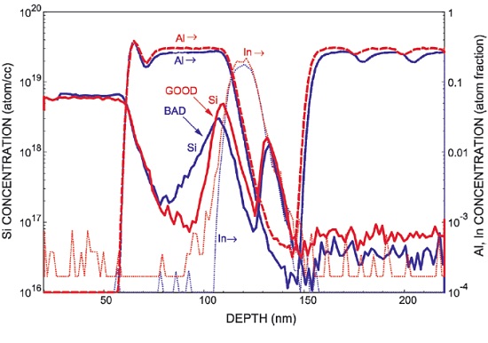
Figure 4 Good and Bad PHEMT Comparison
A similar comparison of the effect of a 1 keV versus 2 keV is shown in Figure 3 for the Si profile in the same sample. In this case, the profiles show little, if any difference; the 2 keV energy could be used to speed the analysis without sacrificing resolution.
In order to illustrate the importance of improved SIMS depth resolution, a low impact energy primary ion beam was used to profile the Si delta layers in GOOD and BAD 300×300 µm2 PHEMT devices. Note that in this case the impact energy was the same for both samples.
Figure 4 shows an overlay comparison of the Si, Al, and In signals in the GOOD and BAD samples. The data show that the first Si delta layer in the BAD sample has diffused more than in the GOOD sample. This difference in diffusion can easily be seen, and the ability to see this difference is a direct consequence of the SIMS depth resolution capability used in this measurement.
Would you like to learn more about SIMS for Compound Semiconductor Devices?
Contact us today for your SIMS profiles for compound semiconductor device needs. Please complete the form below to have an EAG expert contact you.
To enable certain features and improve your experience with us, this site stores cookies on your computer.
Please click Continue to provide your authorization and permanently remove this message.