Particle Analysis of sub-50nm Defects by Auger Electron Spectroscopy
Home » Full Wafer Particle Analysis of sub-50nm Defects by Auger Electron Spectroscopy
In the competitive semiconductor marketplace, rapid development of new semiconductor designs and shrinking design rules drive the need for continuous yield enhancement. As design rules shrink, the critical defect size becomes smaller and the identification of defects becomes more challenging. Correct compositional identification of wafer defects has become vital for optimizing tool performance and can have significant financial impact.
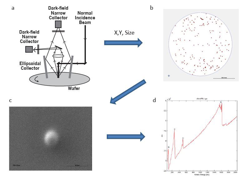
Defects are usually first discovered in an optical detect mapping tool, which typically provides location and sizing information for the defects (Fig. 1a). A map is generated that shows the location of the defects on the wafer (Fig. 1b). Individual defects are then located using the coordinates provided by the particle scanner and an SEM image of the defect is obtained (Fig. 1c). Finally, a compositional analysis is performed (Fig. 1d).
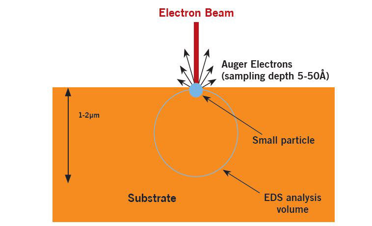
Historically, defects have been analyzed by Energy Dispersive X-Ray Spectroscopy (EDS); however, only a small fraction of the X-rays collected in a standard EDS analysis originate from the defect due to the large sampling volume of the technique.
Figure 2: Comparison of detection volumes, AES vs. conventional EDS
This situation becomes increasingly worse as defects become smaller, which often can lead to inconclusive results. This problem can be mitigated to some extent by using low accelerating voltages and windowless detectors but still leaves only the less reliable low energy spectral lines for analysis.
In contrast, the high surface sensitivity and small analysis volume of Auger Electron Spectroscopy (AES or Auger) makes Auger the ideal technique for the analysis of sub-50nm defects. Since the sampling depth is independent of acceleration voltage, high beam energies can be used to excite all available transitions in the spectrum. The Auger signal is collected mainly from the surface of the defect (Fig. 2) and as a result, the signal contribution from the defect stays nearly constant with shrinking defect size. Auger spectra do also contain some contribution from the substrate due to beam scattering, which can be minimized but not eliminated.
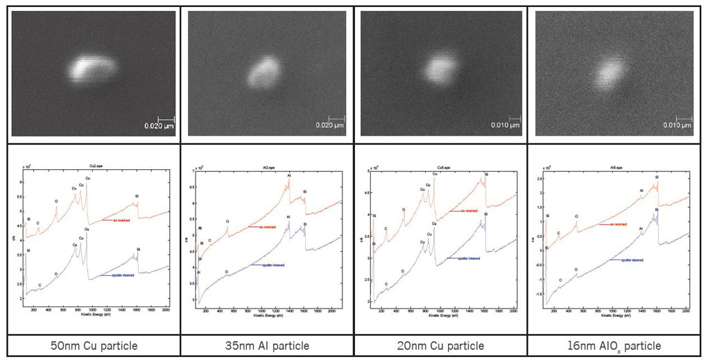
Figure 3
Figure 3 shows some examples of SEM images and Auger spectra data collected from small defects of various sizes of various sizes from 50nm down to 16nm. Excellent sensitivity, as documented by the strong signal intensity, is maintained down to a defect size of only 20nm, with some signal drop-off below this size. Spectra were acquired before and after sputtering.
Would you like to learn more about Particle Analysis by Auger Electron Spectroscopy?
Contact us today for your particle analysis by Auger Electron Spectroscopy needs. Please complete the form below to have an EAG expert contact you.
To enable certain features and improve your experience with us, this site stores cookies on your computer.
Please click Continue to provide your authorization and permanently remove this message.