
A Deep Dive into High Powered Electronics
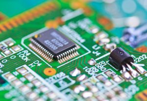
High Powered Electronics are used in a wide suite of applications, from consumer electronics and electric vehicles to railways and power plants and even artificial intelligence.
High Powered Electronics are used in a wide suite of applications, from consumer electronics and electric vehicles to railways and power plants and even artificial intelligence.
We provide a materials analysis study into the comparison between 22 nm node and 7 nm node FinFET technologies, using TEM-based techniques.

TEM, STEM and AC-STEM techniques deliver high resolution images providing a detailed view of a material or product.

Cryo FIB uses a cold sample stage that can be controlled to -135°C making it it more suitable for temperature sensitive materials.
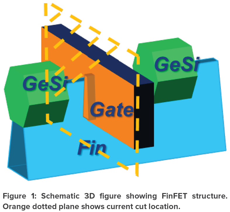
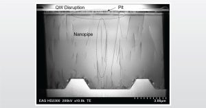
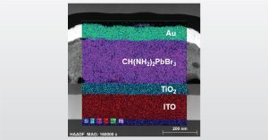
A study into the structure, elemental distribution and crystal orientation of a 22nm FinFET using TEM based analysis techniques
RBS is the one technique where we can really say that the composition and concentration are accurately determined for thin films.
Advanced Surface Analysis using TOF-SIMS on a flat panel display, discovering residue formed during the manufacturing process.

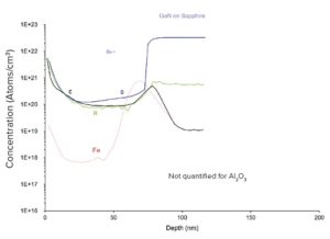
Gallium oxide has the potential to replace or substitute gallium nitride for power conversion in electric trains and vehicles.

Solids fall under two main categories: amorphous and crystalline. These two types of solids have different properties that may be more beneficial for certain products or applications.
In the full webinar we will focus on the PCOR-SIMS Analysis of GaAs pHEMT and GaN HEMT using Secondary Ion Mass Spectrometry
In the full webinar we will introduce analyzing VCSELs with a focus on secondary ion mass spectrometry (SIMS)
June 27, 2024
During this live Ask the Expert event, we will answer pre-submitted questions from our audience regarding Elemental Analysis with Inductively Coupled Plasma (ICP-OES, ICP-MS, LA-ICP-MS). These techniques provide full survey major, minor, trace element analysis, and purity certification for up to 69 measurable elements.
February 12, 2025
During this live Ask the Expert event, we will answer pre-submitted questions from our audience regarding Silicon Carbide for High Powered Electronics. EAG Laboratories has a vast depth of experience analyzing silicon carbide using both bulk and spatially resolved analytic techniques and is the world-leading materials characterization and engineering resource for semiconductor testing.
During this live Ask the Expert event, we will answer pre-submitted questions from our audience regarding materials analysis with various surface contact and optical analytical techniques.
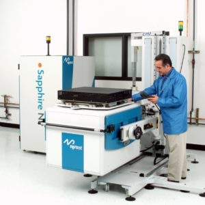
Our wide range of ATE test equipment and experienced team can support from first silicon debug to release
Atomic layer deposition analysis helps you meet ALD specifications for composition, thickness, and crystallinity.
EAG has the timely accurate measurements and information you need to work with analysis of Atomic Layer Deposition thin films
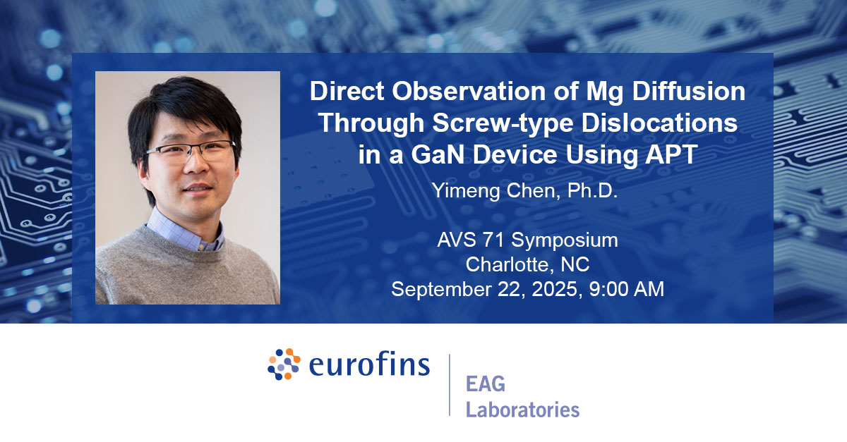
September 21-26, 2025
We are excited to announce that Eurofins EAG Laboratories will be speaking at the AVS 71 Symposium in Charlotte, NC, September 21-26.
Image processing can be used to generate high density critical dimension measurements that allow us to extract the full profile of the interfacial roughness in a multilayer stack.
In the full webinar we introduce Characterization and Failure Analysis of Optoelectronic Materials and Devices
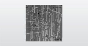
Besides images provided by SEM and TEM, different attachments can be added to reveal crystalline information, including (SEM-EBSD) and TEM (TEM-PED).
In this webinar we introduce Microelectronic Component Product Qualification to understand and consider component reliability.
Electrical AFM can measure the electrical/electromechanical properties of various functional materials and samples. This helps distinguish between conductive and nonconductive areas or polar and nonpolar regions of a device.
The Dual Beam FIB-SEM integrates a focused ion beam with a scanning electron microscope for simultaneous sample prepping and imaging.
In this webinar we introduce Dye and Pry that involves cleaning a sample to remove debris & flux around solder, then exposing it to a red dye.
19th December 2019
EAG Laboratories is proud to help the Global Semiconductor Alliance incubation team assist semiconductor startups

The roughness of a surface and how it interacts with surrounding materials and elements can have a significant impact on material technology and its functionality.

XRF is a non-destructive technique that is used to quantify the elemental composition of materials.

Evaluating Surface and Oxide Composition of Electropolished Stainless Steel for High-Purity Gas Distribution Systems

All materials have trapped gasses inside. Learn how EAG utilizes Evolved Gas Analysis to analyze what gasses are being released.
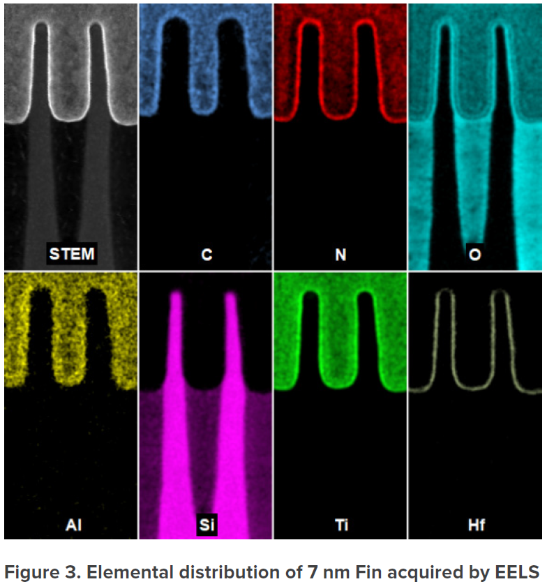
Eurofins EAG Laboratories is proud to announce the addition of Monochromated Electron Energy Loss Spectroscopy (EELS) to its suite of state-of-the-art Transmission Electron Microscopy (TEM) capabilities.

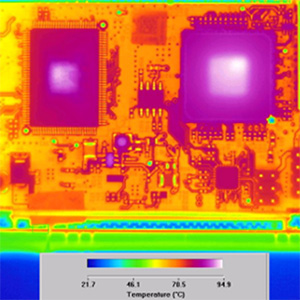
In this webinar we show how EAG troubleshoots electronic system failures using a multidisciplinary approach
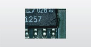
Expert failure analysis will shorten development cycles.
In this webinar we introduce The Failure Analysis of Reliability Testing Samples as applied electronic and semiconductor devices
Speed up your product development cycle with quick and easy FIB edits
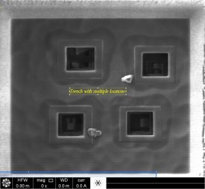
FIB Circuit Edit provides the ability to quickly perform nano-surgury by cutting traces or adding metal connections at the chip level
In this webinar we introduce FIB Circuit Edit which allows the cutting of connections and placement of new lines in a semiconductor die

EAG Laboratories pursues quality in all aspects of our work for customers. ISO certifications and ongoing audits serves many market sectors.

FTIR and Raman are spectroscopy techniques that provide molecular information from various types of materials.

APT is a nanoscale materials analysis technique that provides 3D spatial imaging and chemical composition measurements with high sensitivity simultaneously.
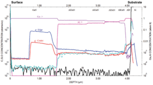
Uncover the invisible architecture of semiconductors with depth profiling using ion-TOF SIMS. This advanced technique reveals layer-by-layer composition in materials like silicon, GaN, and SiC. Learn how Eurofins EAG Laboratories supports your analysis with state-of-the-art tools and world class expertise.

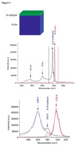
The process of applying both PCOR-SIMSSM and STEM imaging to the same Si-SiGe multilayer sample demonstrates the individual strengths of both techniques and how they can be combined to form a complete understanding of the sample.

Surface cleanliness is critical in how a material or a layer on a product interacts with other surfaces, which in turn can affect its functionality.

LED characterization, from process control to failure analysis to construction analysis, EAG Laboratories supports your LED analysis needs.

Eurofins EAG Laboratories stands ready to assist in the analysis of lithium-ion batteries from the raw material supply chain through to the finished product and eventual recycling.
EAG’s material and microelectronic testing service is dedicated to providing the best information from ensuring the purity of starting materials, to prototype testing of devices in the ramp up towards full-scale production.
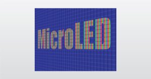
In the full webinar we introduce MicroLED Analysis for improved understanding of III-nitride material properties and growth/device processes
EAG divides FA tasks into three levels. In each level, we employ optimal techniques for device characterization, defect localization, and root cause failure analysis.

Solving CSP qualification testing challenges by addressing key issues and applying specialized processes through EAG know-how.

PFIB differs from traditional FIB in that it uses various gases such as Xe, Ar, oxygen or nitrogen to generate a plasma that is used to remove material from a sample.
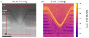
This application note highlights Eurofins EAG’s advanced monochromated EELS capabilities, including bandgap measurement, dielectric function extraction, plasmonic mode characterization, and high precision ELNES chemical state analysis.
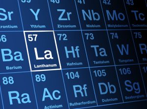
The term ‘rare earth elements’ (REEs) is a misnomer and better refers to the relatively rare ores REEs are extracted from; rare earth elements are all around us!
We help technology innovators translate ideas into realities, improve processes and products, and protect their brands
Semiconductor stress measurements by Raman Spectroscopy helps control problems related to stress control in semiconductor devices, from EAG.

Silicon carbide is increasingly considered a potential replacement for traditional silicon semiconductors due to its superior properties.
Atomic Layer Deposition technology aids in the demand for computational advancement in the microelectronics industry.
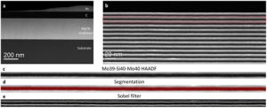
In this application note, we demonstrate our capability to generate a large number of measurements in a single image to determine the roughness of interfaces in a multilayer stack and the roughness correlation across layers.

Technology law covers the use of technology and covers all of the ways that devices and methods of communication impact society.
Through multidisciplinary science and engineering, EAG helps companies translate ideas into technology by supporting R&D, NPI and production.
In this webinar we introduce the Testing of High Speed I/O to validate the devices from characterization to production

PCOR-SIMS was originally developed to analyze Silicon Germanium (SiGe) devices for the communications industry.

Warpage Analysis serves as a valuable tool for measuring the warpage and deformation experienced by products under thermal stresses.

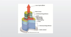
VCSELs have several advantages, such as a higher modulation speed, which make them great for technological innovations.
In the full webinar we will discuss Thin Film Analysis that looks at film composition, thickness, and uniformity.

LA-ICP-MS is a technique that uses direct micro-scale sampling to provide high precision elemental characterization of solid materials.

Automated Test Equipment (ATE) systems are carefully designed to test a wide range of semiconductor devices. EAG provides tailored ATE test solutions to meet the unique needs of clients.
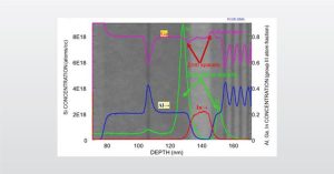
HEMTs characterization using SIMS helps to uncover troublesome impurities, optimize epitaxial layer growth and aid failure analysis
High Depth Resolution Analysis will play a very important role in the electronic device industry as devices become smaller and smaller.
EDS and EELS can be coupled with SEM, STEM and TEM to determine the elemental composition, spatial distribution and segregation of elements.

In our interconnected and changing world, it is important to know how to respond to potential electronic system failures.
From semiconductor dopant profiling to contamination investigations, SIMS plays a critical role in solving some of the most demanding analytical challenges. Explore the applications where SIMS provides unique insights.
To enable certain features and improve your experience with us, this site stores cookies on your computer. Please click Continue to provide your authorization and permanently remove this message.
To find out more, please see our privacy policy.