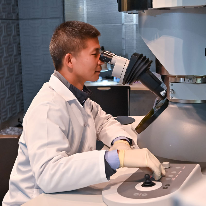
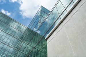
For example, the quantum wells in LEDs can be extremely thin where we would need AC-STEM to see irregularities between quantum well – barrier interfaces. This is beneficial for compound semiconductors. Even for the thicker layers in compound semiconductors, you can obtain images with atomic number related contrast which can be more clearly seen observed using STEM. For failure analysis related jobs, we may go straight to STEM to pinpoint a failure. There are so many factors to keep in mind. What if you still don’t know which technique to use? That’s where we come in!
At Eurofins EAG, we are your trusted partner in advanced microscopy analysis. We are one of the few commercial labs to offer AC-STEM services along with a vast array of complementary analytical techniques. With our years of experience working with a multitude of materials and industries, we can help determine the best suited techniques for your project.
Contact us today to learn how we can help you on your next project.