ICP-OES Webinar
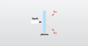
In this webinar we will focus on Inductively Coupled Plasma Optical Emission Spectroscopy (ICP-OES), and ICP-MS

In this webinar we will focus on Inductively Coupled Plasma Optical Emission Spectroscopy (ICP-OES), and ICP-MS
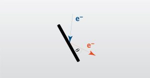
This webinar will focus on Electron Backscatter Diffraction (EBSD) and Electron channeling contrast imaging (ECCI)
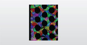
In this webinar we introduce Precession Electron Diffraction (PED) which has been essential to nano-scale structural analysis
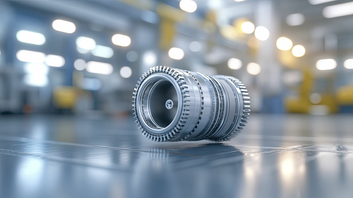
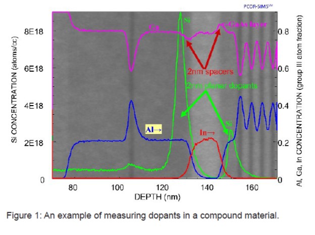
Explore the hidden risks of impurities during manufacturing and how advanced methods like GDMS and ICP-MS help safeguard critical components.
To enable certain features and improve your experience with us, this site stores cookies on your computer. Please click Continue to provide your authorization and permanently remove this message.
To find out more, please see our privacy policy.