Optimizing 2-D Electron Density in pHEMTs Using Secondary Ion Mass Spectrometry
Home » Optimizing 2-D Electron Density in pHEMTs Using Secondary Ion Mass Spectrometry
In a heterostructure FET (HFET) a heterojunction interface between an n-AlGaAs donor layer and an undoped InGaAs layer leads to a change in the conduction and valence bands at the interface that creates a sharp potential well in which donor electrons can reside under a forward gate bias condition.
The depth of this well is determined by the exact composition of the two hetero materials on either side of the interface.
Injection of electrons from the AlGaAs layer into the InGaAs layer results in electrons being separated from the Si donor ions and confined in a thin layer in the InGaAs near the interface. This thin plane of electrons is highly mobile and forms a two dimensional electron gas (2DEG) layer for transconductance of current between the source and drain of the device.
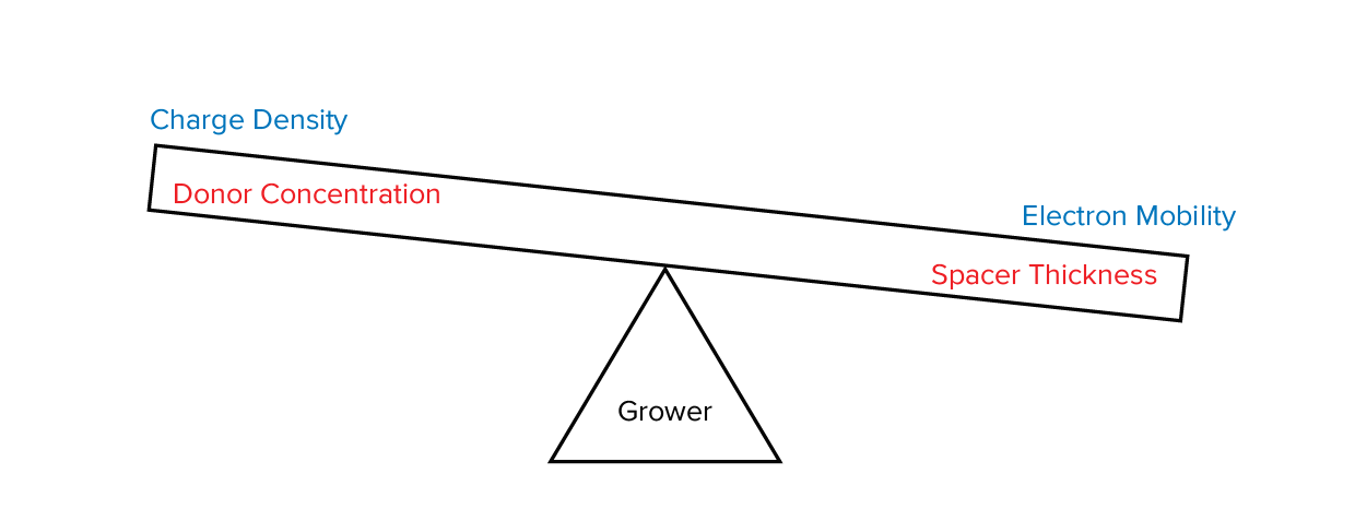
Typically, to aid in separating the electrons from the donor ions (which improves electron mobility due to decreased scattering) the grower typically incorporates a very thin AlGaAs or GaAs “spacer” layer between the Si donor atoms (present as a delta doping spike in the AlGaAs) and the InGaAs channel region. PHEMT growers typically target certain electron mobility and charge density, which can be accomplished, respectively by spacer layer thickness and doping concentration.
One must be careful, however, because too great a spacer layer thickness will decrease the number of electrons able to tunnel from their donor atoms across the heterostructure interface and into the InGaAs channel thus reducing the charge density in the 2DEG. A thinner spacer layer will not sufficiently separate the electrons from the donor atoms and increased scattering of the electrons off these donor atoms will result in decreased electron mobility. However, an increase in charge density would result.
Likewise, the grower must be careful in growing the Si deltadoping spikes. Too low a doping level will result in decrease electron density in the 2DEG layer, while too high a doping level will result in increased electron scattering from the Si donor atoms which, as mentioned above, results in decreased electron mobility. So the grower has a “balancing act” to perform in fabricating these structures. See figure 1.
Adding to the complication is that reaching the targeted spacer thickness can be difficult because the methods typically used to fabricate pHEMTs can be difficult to control. Because the spacer layer (25 – 40 Å) is so thin, brief growth durations are required, and what is more, they occur between critical actuation of shutters and valves that are pausing the growth of the matrix elements as well as turning on and off the dopant. The subsequent flux decays are dependent on cell conditions such as geometry, temperature, pause times, carrier gas flow, etc which are all difficult to characterize.
Ultimately, the PCOR-SIMSSM profile can provide the information needed by the grower/designer regarding doping levels and spacer layer thicknesses that are actually achieved in a growth run. This factually helps the grower to know where he exactly stands in reference to the targeted values.
DISCUSSION
Crucial to the success at using SIMS for this application is its ability to determine accurately:
- III-V material compositions (for energy band optimization)
- Doping density
- Spacer layer thickness
The vast number of combinations of Group III and Group V materials that are commonly used in modern III-V devices creates severe problems for the SIMS in achieving these requirements. Large numbers of standards needed to achieve quantitative accuracy, and many supportive techniques must be brought to bear to confirm the SIMS results. The efforts of the EAG for this very challenging area of materials analysis are met by Point-by- Point-Corrected SIMS (PCOR-SIMSSM).
PCOR-SIMSSM accurately measures the areal density of the Si doping spikes and accurately determines layer thicknesses by taking into account the change in Si SIMS sensitivity and sputtering rate with AlGaAs and InGaAs composition.
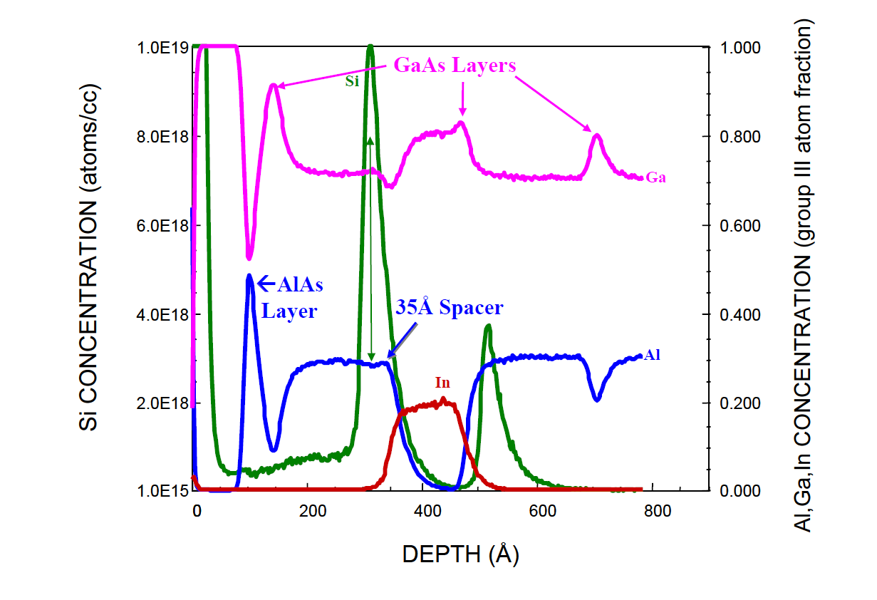
Figure 2 demonstrates the usefulness of PCOR-SIMSSM for optimizing the channel region of a pHEMT device in which the 2DEG resides. This particular device a double-heterostructure (DH) FET where the conducting channel (InGaAs in this example) is bounded on both sides by AlGaAs confinement layers with doping being supplied from two Si planar doping layers, one on either side of the channel. The effect of the confinement is to increase the effective carrier velocity in the channel.
The complication is then to manage simultaneously the charge transfer from both sides of the channel. In fact, the effective contribution to the charge from each side is a function of the spacer and the Si dose. The ultimate contribution ratio is not necessarily the same as the nominal atomic concentration of dopant (Si). In addition, the behavior is not linear over the generally used range of doping doses. The matter gets further complicated when an asymmetric configuration is used; namely when the spacer thicknesses are not the same.
The depth resolution of the analysis reveals the spacer layers, as well, even though they are as thin as 35Å. The differences in sputter rates between AlGaAs, InGaAs and GaAs are corrected at each point. This is necessary for pHEMT structures for accurate evaluation of the spacer layer, which corresponds to the AlGaAs layer thickness between the Si spiked layer and the start of the InGaAs layer (i.e. half rise in In profile). By utilizing the Si profiles, the AlGaAs layers ranging from a few tens to few hundreds of Angstroms can be accurately segmented between the upper AlGaAs layer and the lower spacer layer. Other analytical techniques may identify the total AlGaAs layer thickness, but SIMS is unique in being able to unambiguously divide this layer into its two halves.
Figure 3 demonstrates the ability of PCOR-SIMSSM to measure the spacer layer thickness with sufficient accuracy to establish the quantitative relationship between spacer layer thickness and electron mobility. As stated in the introduction, mobility depends on the spacer layer thickness (as well as other things). We wish to show that, other structure variables being unchanged, SIMS can measure a change in spacer layer thickness that would be consistent with a measured change in mobility. The physical separation between Si donor ion and electron prevents unwanted Coulombic scattering resulting in high e-velocities in the active layer (and thus higher electron mobility.
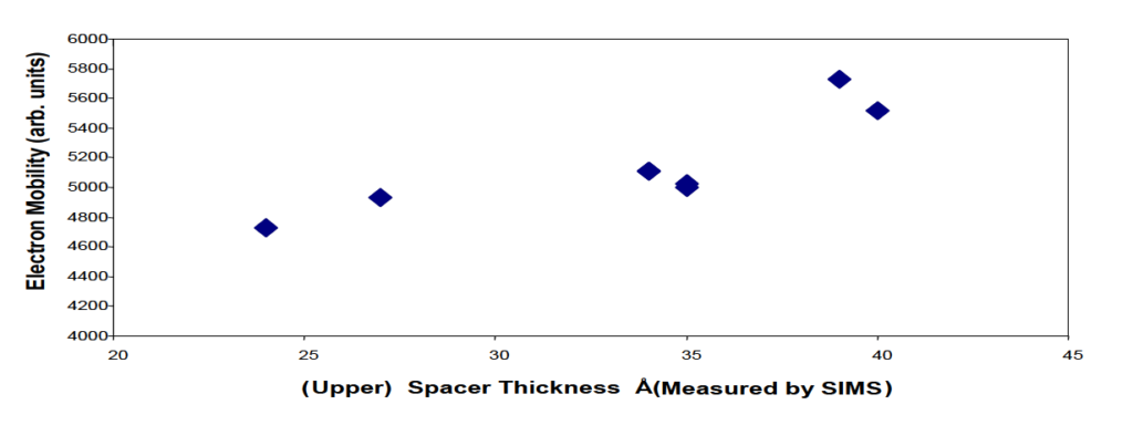
Figure 3 demonstrates the ability of PCOR-SIMSSM to measure the spacer layer thickness with sufficient accuracy to establish the quantitative relationship between spacer layer thickness and electron mobility. As stated in the introduction, mobility depends on the spacer layer thickness (as well as other things). We wish to show that, other structure variables being unchanged, SIMS can measure a change in spacer layer thickness that would be consistent with a measured change in mobility. The physical separation between Si donor ion and electron prevents unwanted Coulombic scattering resulting in high e-velocities in the active layer (and thus higher electron mobility.
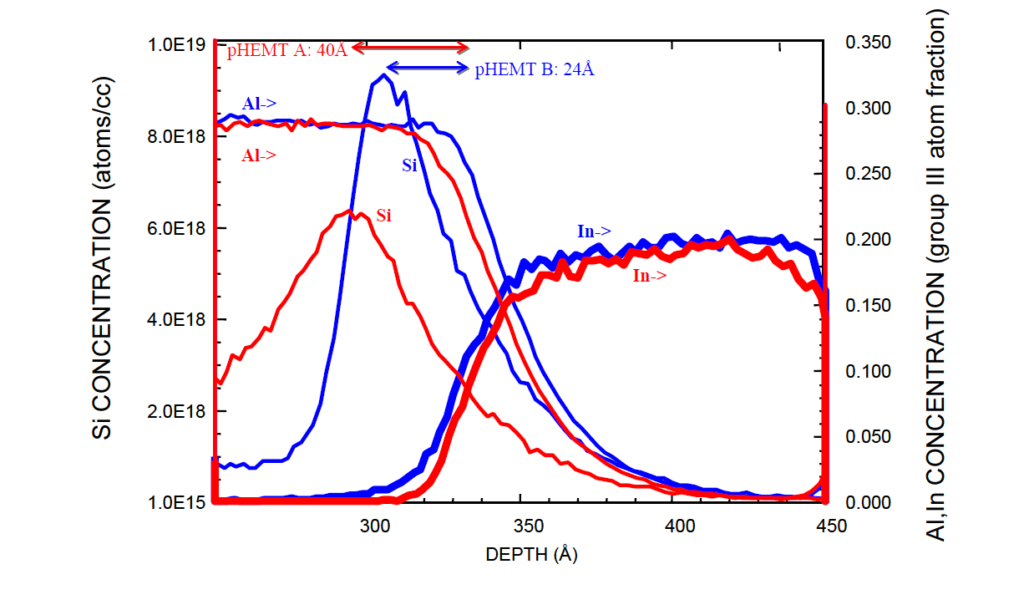
Examples of SIMS depth profiles from two of these samples are shown in Fig. 4.
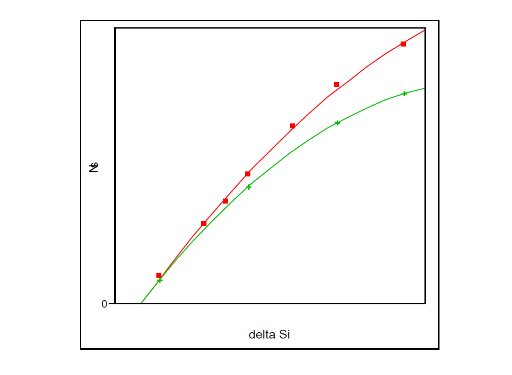
A similar relationship can been seen in figure 5 between the amount of electron charge density in the pHEMT active layer (InGaAs) and the areal density of Si donors in the Si delta-doped layer. During application of a forward bias at the gate electrode, the amount of electrons that can charge transfer from the donor atoms into the (InGaAs) active layer is dependent on the amount of Si donor atoms present in the Si delta-doped layer.
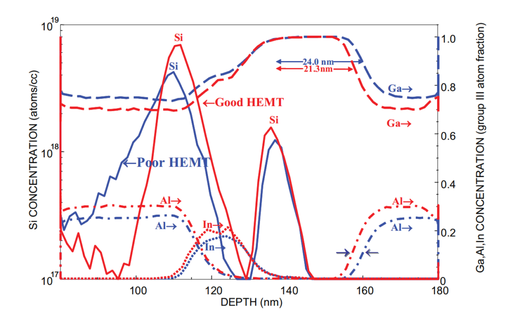
In addition to these examples of using PCOR-SIMSSM for process development, PCOR-SIMSSM can also be used for failure analysis of pHEMTs. Figure 6 shows PCOR-SIMSSM profiles in the active region of a “good” and a “poor” pHEMT. For these two PHEMT structures, note the difference in peak Si concentration in the top Si delta-doped layer. The increased apparent diffusion of the top Si spike towards the surface can be the result of either too high a growth temperature or imperfect switching off the dopant source for the upper delta doping (but most likely both). Also in Fig. 6, note the diffusion of the Si doping spike away from the InGaAs channel region. This reduces the number of donor atoms that reside close enough to the conduction band offset (AlGaAs/InGaAs interface) to allow a sufficient number of electrons to tunnel into the channel region resulting in degraded device performance as it will require more atomic Si to achieve the needed charge but this is undesirable because of increased electron scattering. It is also possible that a broader Si delta distribution could lower the breakdown voltage.
CONCLUSION
In conclusion, we have shown how PCOR-SIMSSM can be used by the grower of III-V high-speed transistor structures by helping to optimize the “balancing act” tradeoff of structural features that determine electron mobility and electron change density in the channel region, both or which affect device performance. Despite the accessibility of some powerful techniques to the grower, the assessment of the device in the vicinity of the channel region, namely the interfacial region, is better and most factually assessed by SIMS. This enables the grower to determine exactly what is happening to cause the observables by other testing means.
Would you like to learn more about Optimizing 2-D Electron Density in pHEMTs?
Contact us today for your optimizing 2-D electron density in pHEMT needs. Please complete the form below to have an EAG expert contact you.