IGA Webinar
This webinar will focus on Instrumental Gas Analysis (IGA) that measures gas-forming elements present in solid materials.

This webinar will focus on Instrumental Gas Analysis (IGA) that measures gas-forming elements present in solid materials.

As a trusted partner in the consumer electronics industry, we are ready to meet the evolving industry needs, advancing innovation and excellence.
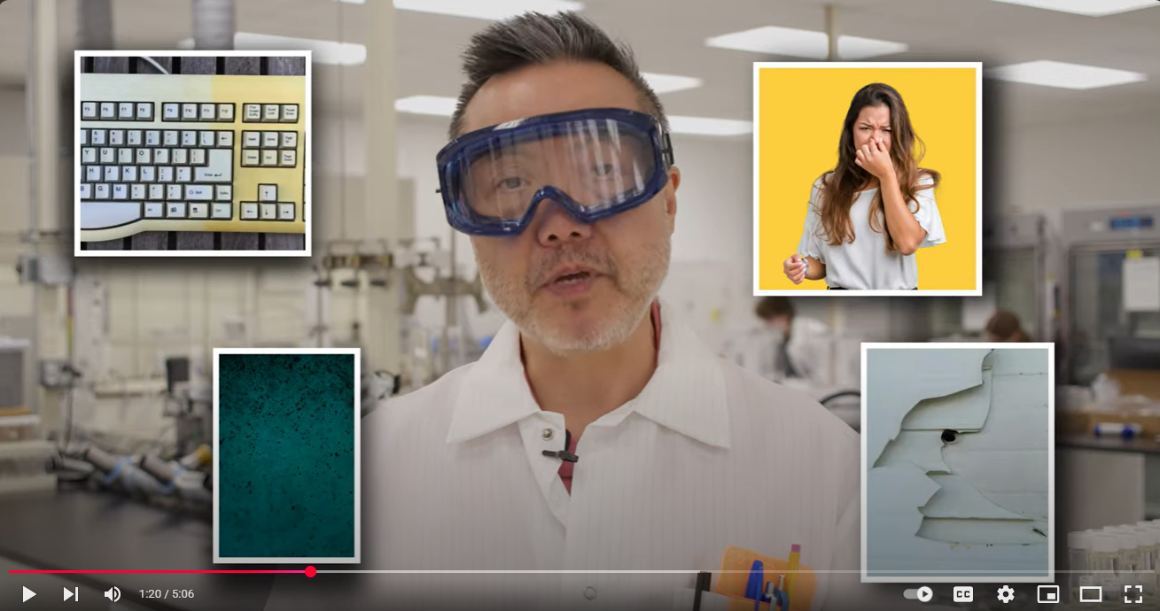
Join us “In the Lab” to learn how investigative analytical chemistry can help solve your product or manufacturing line problems!
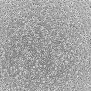
In Vitro testing uses cell-based biological models instead of animals or humans.
To enable certain features and improve your experience with us, this site stores cookies on your computer. Please click Continue to provide your authorization and permanently remove this message.
To find out more, please see our privacy policy.