A materials analysis study into FinFET technology
We provide a materials analysis study into the comparison between 22 nm node and 7 nm node FinFET technologies, using TEM-based techniques.
We provide a materials analysis study into the comparison between 22 nm node and 7 nm node FinFET technologies, using TEM-based techniques.
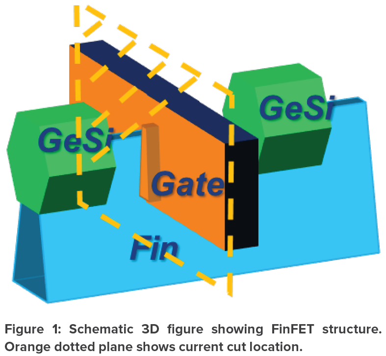
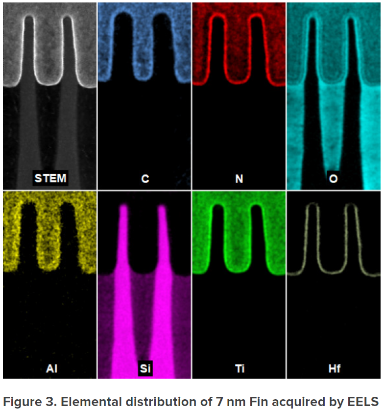
A study into the structure, elemental distribution and crystal orientation of a 22nm FinFET using TEM based analysis techniques
AC-STEM with Secondary Electron (SE) imaging provides the unique capability of evaluating specimen surface morphology with atomic-resolution.
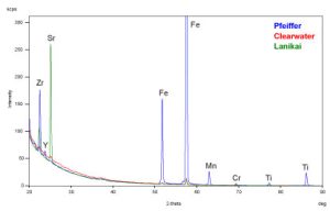
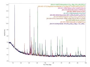
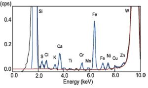
WDXRF and XRD are two powerful tools that allow us to obtain detailed characterization of materials, covering both the elemental composition and crystalline phases present.
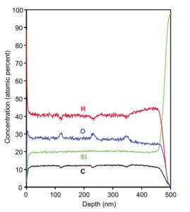
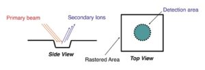
SIMS depth profile characterization provides accurate quantification for all measured species and matrix using our unique reference materials
Uncover the invisible architecture of semiconductors with depth profiling using ion-TOF SIMS. This advanced technique reveals layer-by-layer composition in materials like silicon, GaN, and SiC. Learn how Eurofins EAG Laboratories supports your analysis with state-of-the-art tools and world class expertise.
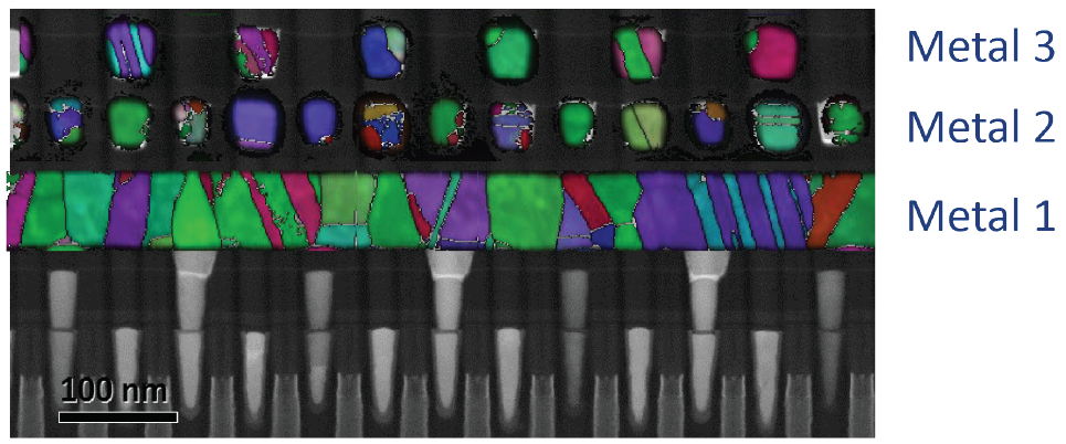
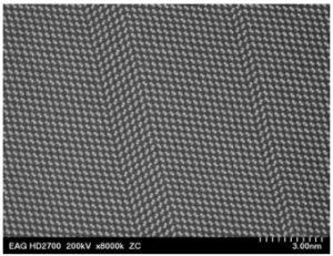
Examples of crystal grain orientation mapping and strain mapping in 7nm EUV technology IC chip and strained Silicon
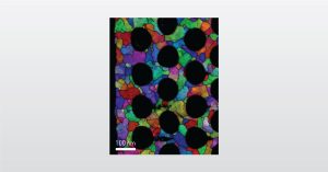
Microdiffraction can be used to identify crystalline inclusions in glass, look at film texture in a test pad on an integrated circuit, identify a single particle found in an air filter, or to identify the phosphor used in an LED.
In this webinar we introduce Precession Electron Diffraction (PED) which has been essential to nano-scale structural analysis
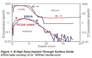
PCOR-SIMS is an EAG proprietary technique that can measure layer thickness, composition, and doping profiles.
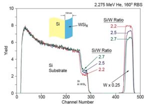
View typical RBS services results from EAG used for compositional thin film analysis for semiconductors, optimal coatings and more.
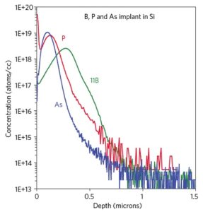
SIMS services from EAG is featured in this technique note, including sample data, showing how SIMS detects low concentrations of impurities
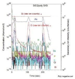
Survey-SIMS Depth Profiles analyze for dopants & impurities in a material without having prior knowledge in the structure being evaluated.
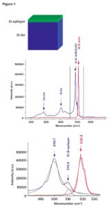
Semiconductor stress measurements by Raman Spectroscopy helps control problems related to stress control in semiconductor devices, from EAG.

Silicon carbide is increasingly considered a potential replacement for traditional silicon semiconductors due to its superior properties.
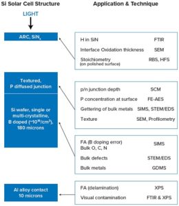
Silicon wafer solar cells and the analytical techniques used to investigate failures, bulk defects and other materials characterization.
EAG’s SIMS Analysis Individual SiC Particles using a special sample preparation technique eliminates contributions from surface contamination
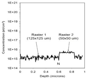
Raster change technique is used for SIMS measurement of very low levels of nitrogen in Silicon carbide by EAG Laboratories.
Secondary ion mass spectra measured by SIMS may not always provide information from the target element alone.
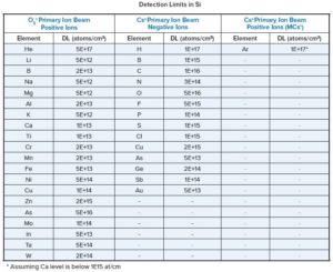
SIMS Detection Limits of Selected Elements in Si and SiO2 Under Normal Depth Profiling Conditions SIMS is a powerful analytical technique which allows detection of all
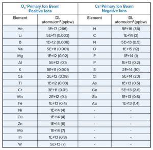
SIMS detection limits of selected elements in Silicon, providing a a list of detection limits for typical dopants and impurities
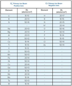
SIMS detection of all elements from H to U with excellent sensitivity. The table provides detection limits for impurities in a SiC matrix.
Silicon Carbide SIMS Measurements provide valuable data for process control and problem solving in wafer growth and device manufacturing.
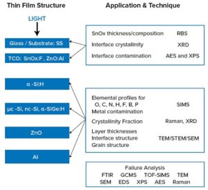
Surface analysis lab techniques on α-Si thin film PV, microcrystalline Si, nanocrystalline Si, amorphous SiGe, & microcrystalline SiC
In this webinar we will introduce the principles of Transmission Electron Microscopy (TEM) with a focus on real-world problem-solving.
TXRF AND SURFACESIMS.XP is the total solution for surface contamination measurements on semiconductor surfaces, from EAG Laboratories.
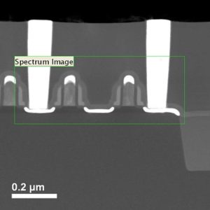
Two-dimensional mapping of matrix elements in electronic devices is discussed, as provided by STEM and EELS techniques from EAG Laboratories.
Transmission Electron Microscopy is often used to evaluate defects in crystals, but not all defects can be observed with TEM

XRD analysis can be used on many scientific and technology-based applications where you may want to identify the crystalline material in a very small area or volume, such as glass defects or inclusions, integrated circuits, LEDs and more.
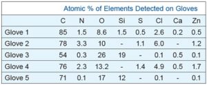
XPS Analysis of Disposable Gloves assesses materials exposed during product manufacturing to make sure contamination is not introduced.
To enable certain features and improve your experience with us, this site stores cookies on your computer. Please click Continue to provide your authorization and permanently remove this message.
To find out more, please see our privacy policy.