The Total Solution For Surface Contamination Measurements
Home » The Total Solution For Surface Contamination Measurements
Ultra-clean surfaces are critically important to successful processing of semiconductor devices. Device failure can often be attributed to surface contaminants such as transition metals and alkali atoms. In order to control contaminants, it is necessary to identify and quantify them.
Utilizing both TXRF and SURFACESIMS. XP provides the total solution with the best value for surface contamination measurements on semiconductor surfaces.
FEATURES OF TXRF
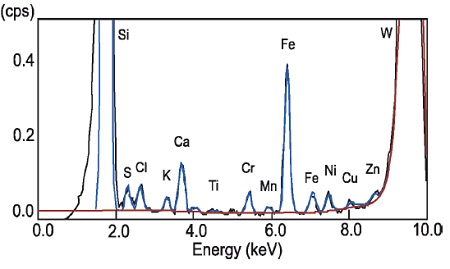
Survey technique; detection of elements from S to U.
Non-destructive, automated analysis in a clean room environment.
Whole wafers 100 – 300 mm. Smaller wafers down to 50 mm may be mounted for analysis.
Large analysis area (10 mm diameter) at a glancing angle below the critical angle.
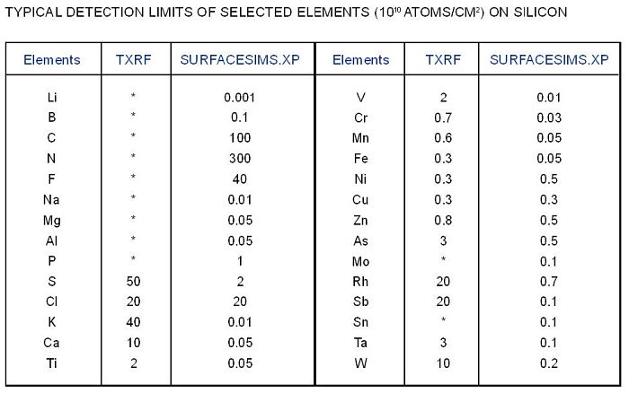
Detection limits ranging between 109-1010 atoms/cm2 for most metals.
As a survey technique, TXRF provides high sensitivity multi-element surface contamination measurements at low cost.
FEATURES OF SURFACESIMS.XP
Element-specific detection of all elements and isotopes, especially light elements (H-S) where TXRF has poor detection efficiency.
ASTM methods (F1617-98) for Al, Na, K and Fe contamination on silicon and epi substrates.
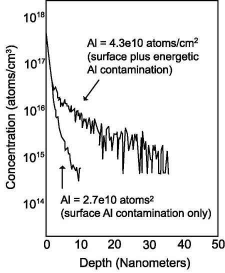
Measurement of near surface depth distributions, providing both surface and in depth detection of contamination.
Small analysis areas (minimum 50×50 µm2) – very useful for device applications and for navigating measurements between airborne particles
Detection limits ranging between 108-109 atoms/cm2 for most metals.
Long term precision: ~10% RSD.
Applicable substrates: Si, SiO2, SiC
SURFACESIMS.XP provides (1) areal densities of surface contaminants and (2) information about the near surface depth distribution of contaminants. This represents an important advantage over TXRF, VPD-AAS, and VPD-ICPMS.
Figure 2 SURFACESIMS.XP depth profiles of Aluminum in Si
* These elements cannot be detected by TXRF or cannot be measured at practical levels. In some cases, spectral interferences prevent detection at low levels.
REFERENCES
Correlation between SURFACESIMS and TXRF measurements of surface metal contamination on silicon, S. P. Smith, J. Metz and P. K. Chu, in Secondary Ion Mass Spectrometry (SIMS XI), edited by G. Gillen, R. Lareau, J. Bennett and F. Stevie. (John Wiley & Sons, Chichester, 1998) pp. 233-236.
Would you like to learn more about Surface Contamination Measurements?
Contact us today for your surface contamination measurement needs. Please complete the form below to have an EAG expert contact you.
To enable certain features and improve your experience with us, this site stores cookies on your computer.
Please click Continue to provide your authorization and permanently remove this message.