Secondary Ion Mass Spectrometry Survey Depth Profile
Home » Secondary Ion Mass Spectrometry Survey Depth Profile
Secondary ion mass spectrometry (SIMS) is a powerful analytical tool for in-depth analysis of thin films. What sets SIMS apart from other surface-analysis techniques is its extremely high sensitivity (ppb levels for most elements).
However, heretofore, this has come at a price. You needed to know what dopants or impurities were in the sample structure before the analysis could be started. This came about because of the nature of acquiring depth profiling data with a “traditional” SIMS depth-profiling tool where the chosen elements are monitored sequentially as the surface is sputtered with the primary ion beam.
This is the case with magnetic sector-based and quadrupole-based mass spectrometers. While the chosen elements are monitored, all other elements go undetected. It is thus incumbent of the analyst to have a thorough knowledge the possible elements of interest so that they can be monitored in the analysis.
However, many times this is not possible. An investigator will present a sample to the SIMS analyst saying: “My material doesn’t work. Why? What’s in it?” without giving the analyst any suspect elements for which to analyze.
Often an experienced analyst can rely on his or her accumulated knowledge to choose elements which might be responsible for the material’s failure, but this is no guarantee that he or she has chosen correctly. The elements that are responsible for the failure may go undetected.
PRINCIPLES
A time-of-flight based SIMS tool gets around this need to know what is in a sample before beginning the analysis. In a time-of-flight instrument, the surface is probed with a pulsed, extremely low primary ion flux to generate the secondary ion signal. The surface is virtually “un-sputtered” during data acquisition. For each pulse of primary ions, a complete mass spectrum is acquired detecting all the elements present in the sample. Once sufficient signals are accumulated in this virtually non-sputtering mode, another ion beam is used to sputter away material to expose a new depth to be probed by the pulses of primary ions. This method of acquiring a depth profile is called a “Survey Depth Profile” because it provides a complete survey analysis of the sample at every depth interval.
One does not have to know what is in the sample before analyzing it because every element is detected at every depth interval. In addition, the decoupling of the sputter-removal of material from the secondary ion generation leads to great advantages when analyzing multi-layered samples where impurities at interfaces might be particularly important. All the elements present at the interface are detected, and sputter-removal of the surface can be halted at the interface and more data accumulated to obtain better a better detection limit. With “traditional” SIMS depth-profiling tools where sputtering is continuous through an interface, when detecting one impurity at an interface, another element-of-interest that is present might be missed because by the time the mass spectrometer is tuned to it, the sputtering may have passed through the interface where that element might have been. In that way, a false negative result may be reported. This cannot happen in a Survey-SIMS depth profile.
EXAMPLES
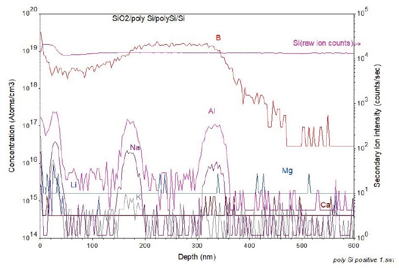
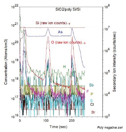
Figures 1 and 2 show Survey-SIMS depth profiles of a thin film layer structure of SiO2/poly-crystalline Si on a crystalline Si substrate.The data were acquired in two separate analyses; one of electronegative species (fig. 1); and one of electropositive species (Fig. 2). For achieving optimum detection limits, these two element-groups must be measured separately.
In figure 1, the oxygen profile (plotted in intensity with respect to the right y-axis) shows the presence of the SiO2 layer on the top of the structure. However, additionally, the oxygen profile shows oxide contamination at the poly-Si/crystalline-Si interface and in the middle of the poly-Si layer. This is indicative of a two-step deposition process for the poly-Si. The arsenic profile (plotted in atoms/cc with respect to the left y-axis) shows that this in-situ As doping also accumulated at the same two interfaces as well as at the SiO2/poly-Si interface. There is also evidence that some of the As has diffused out of the heavily-doped poly-Si layer into the underlying Si substrate.
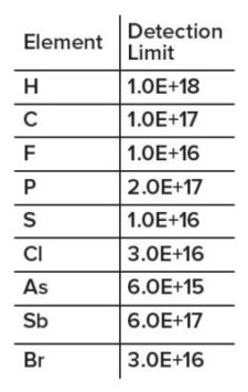
Fluorine and carbon are also detected that all three of these interfaces. The caption for fig. 1 lists the detection limits for the electro negative elements that are commonly found in this kind of material system.
Figures 2 shows profiles for electropositive elements acquired on the same structure. Lithium, Na, K and Al contaminants are detected at the same interfaces where F was detected in Fig. 1.
Alkali-element contamination can be particularly deleterious to device performance, leading to C-V shifts in devices if these mobile species find their way into the active device layers. The Al present at these interfaces could be indicative of contamination from Al metallization layers deposited at these points in the process flow. The alkali contamination could be come from the resist used to pattern the device at these points in the processing.
Boron is also detected in the structure. The B level in the poly-Si is important because, while lower in concentration than the As, the B will nevertheless counter-dope the As which is the opposite dopant type, thus reducing the net n-type doping of the As.
The boron diffusion into the Si substrate will also affect the net electrical doping in the substrate under the poly-Si where both As and B are present.
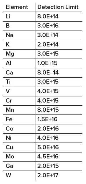
All other electropositive elements that were quantified were not present. Their detection limits are listed in the captions for the figures.
SUMMARY
Survey-SIMS Depth Profiles provide a way to analyze for dopants and impurities in a material without having prior knowledge of their presence in the structure being evaluated. By analyzing for both electronegative and electropositive elements (in two, separate analyses), one can detect all elements in the periodic table with excellent depth resolution and high sensitivity.
Once the elements of interest are identified, one may wish to profile these with a “traditional” magnetic sector or quadrupole SIMS depth-profiling tool to obtain even better detection limits, especially for atmospheric contaminants.
Would you like to learn more about Secondary Ion Mass Spectrometry Depth Profile?
Contact us today for your Secondary Ion Mass Spectrometry survey depth profile needs. Please complete the form below to have an EAG expert contact you.