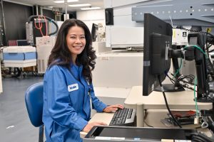
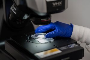
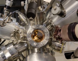
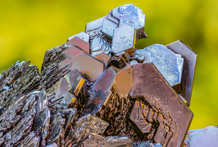
Silicon Carbide - A Powerful Semiconductor for the Future

Lately, semiconductors like silicon carbide, gallium nitride, and gallium oxide have been trending in the news – but what exactly is a semiconductor?  And why does silicon carbide offer advantages over the traditionally dominant semiconductor silicon?  In this blog, we explore the properties of silicon carbide and applications like power electronics in vehicles and advanced sensors for extreme conditions in which it could displace silicon.

What is Silicon Carbide?

Silicon carbide (SiC), also known as carborundum, is a refractory compound and semiconductor which has been widely produced for industrial applications since the late 19th century.  Some of these applications include abrasive and cutting tools, composite vehicle armor and ballistic plates for body armor, high-performance automobile brake disks, and the coating of advanced “TRISO” 

silicon carbide

radioactive fuel kernels used in some fission reactors.  However, it is mainly the semiconducting properties of silicon carbide, rather than its refractory and abrasive characteristics, that has this material making headlines today.

Semiconductors are materials that alternately behave as conductors (like copper electrical wiring) or insulators (like the polymer insulation on those wires). One of the key properties that determines the usefulness of semiconductors for a particular application is its bandgap; this is the amount of energy required to switch between insulating and conducting states. The traditional semiconductor silicon has a fairly small bandgap of around 1.12 electron-volts (eV), while silicon carbide has a bandgap of about 3.26 eV (Wolfspeed). A wide bandgap (WBG) material can move electrical energy more efficiently than smaller bandgap semiconductors. This makes silicon carbide especially useful for power electronics like traction inverters in electric vehicles and DC/DC converters for electric vehicle chargers and air conditioners (Zeeburg). According to the market research and strategy consulting company Yole Group, the device market for silicon carbide is anticipated to grow from ~$1 billion USD in 2021 to greater than ~$6 billion USD by 2027 (Chiu and Dogmus, Ph.D.).

The Advantages of Silicon Carbide

Silicon carbide is increasingly considered a potential replacement for traditional silicon semiconductors due to its superior properties.  While silicon semiconductors have been the dominant material in the electronics industry for many years, SiC offers several advantages that justify its higher cost when deployed in demanding applications like power electronics for terrestrial electric vehicles or instruments on rovers and probes used in space exploration (Mantooth, Zetterling and Rusu).

silicon carbide
  1. Higher temperature capability: SiC can operate at much higher temperatures than silicon, often up to 400 degrees C and potentially up to 800 degrees C, allowing for more efficient electronic devices that can handle extreme conditions without significant performance degradation. This impressive capability is due to the high thermal conductivity of SiC and the low intrinsic concentration of charge carriers.  High thermal conductivity means that a SiC transistor can use a much smaller heatsink than an equivalent silicon chip or can use a comparable heat sink and tolerate much more heat.  Low concentration of charge carriers at room temperature means that SiC can tolerate greater electrical load before thermally liberated electrons add to the intrinsic charge carriers, flooding the transistor, and locking it in the “on” position (conducting state).
  2. Higher breakdown voltage: SiC has a breakdown voltage roughly eight times greater than that of silicon (~300 kV/cm versus 2400 kV/cm), meaning that it can

withstand higher voltages before experiencing unpredictable conduction behavior and potentially catastrophic failure.

3. Smaller form factor: This advantage follows from the higher breakdown voltage and thermal conductivity of SiC relative to silicon. If a silicon and a silicon carbide transistor were each designed to withstand up to the same breakdown voltage, the traditional silicon transistor would need to be much larger than the SiC transistor.  The smaller SiC transistor could have as little as 0.25-0.5% as much “on” resistance as the larger silicon transistor.   This property enables the design of more efficient and compact power electronic systems with lower power losses.

4. Higher switching frequencies: The smaller form factor of SiC transistors and consequent higher switching frequency enables the design of lighter weight and less expensive inductors and capacitors for use in a power converter like those used to charge EV batteries.

EAG Expertise in Analyzing SiC

EAG Laboratories has a vast depth of experience analyzing silicon carbide using both bulk and spatially resolved analytic techniques.  Silicon carbide can be doped with various elements to manipulate its electro-thermal characteristics.  For example, silicon carbide can be doped to an n-type semiconductor by adding nitrogen or phosphorous or can be doped to a p-type semiconductor through the addition of beryllium, boron, aluminum, or gallium.  Furthermore, electronic mobility and breakdown voltage are determined by the concentration of dopants in SiC. Verifying the concentration and spatial distribution of dopants in silicon carbide, as well as ensuring that undesirable contaminants are absent, is key to producing high-functioning semiconductors. 

Bulk techniques applicable to SiC include Glow Discharge Mass Spectrometry (GDMS) and X-Ray Fluorescence Spectroscopy (XRF) on solid samples and Inductively Coupled Plasma-Optical Emission Spectroscopy (ICP-OES) and ICP-Mass Spectrometry (ICP-MS) on digested or leached samples.  Laser Ablation-Inductively Coupled Plasma-Mass Spectrometry (LA-ICP-MS), Laser Induced Breakdown Spectroscopy (LIBS), and Scanning Electron MicroscopyEnergy Dispersive Spectroscopy (SEM-EDS) are capable of uncalibrated, semi-quantitative, and fully quantitative elemental measurements, as well as  chemical mapping (imaging of elemental distribution) on solid samples.

Contact EAG today to share your silicon carbide-related objectives and we’ll recommend the most relevant analytic technique for your needs, as well as options for complementary analyses and expert interpretation to create deeper insight.  EAG doesn’t just make measurements; we provide solutions.

More content you might like...

To enable certain features and improve your experience with us, this site stores cookies on your computer. Please click Continue to provide your authorization and permanently remove this message.

To find out more, please see our privacy policy.