A materials analysis study into FinFET technology
Home » A materials analysis study into FinFET technology
7 nm FinFET (Fin field-effect transistor) process technology was introduced to semiconductor manufacturing mass production in 2018, following 10 nm node in 2016, 14 nm node in 2014 and 22 nm node in 2012[1]. While the naming of process nodes is not directly related to any measurable distance on a chip, 7 nm process technology provides shrink down transistors and thus offers improvement in silicon area utilization and power efficiency. In this application note, we provide a materials analysis study into the comparison between 22 nm node and 7 nm node FinFET technologies, using TEM-based (Transmission Electron Microscopy) techniques.
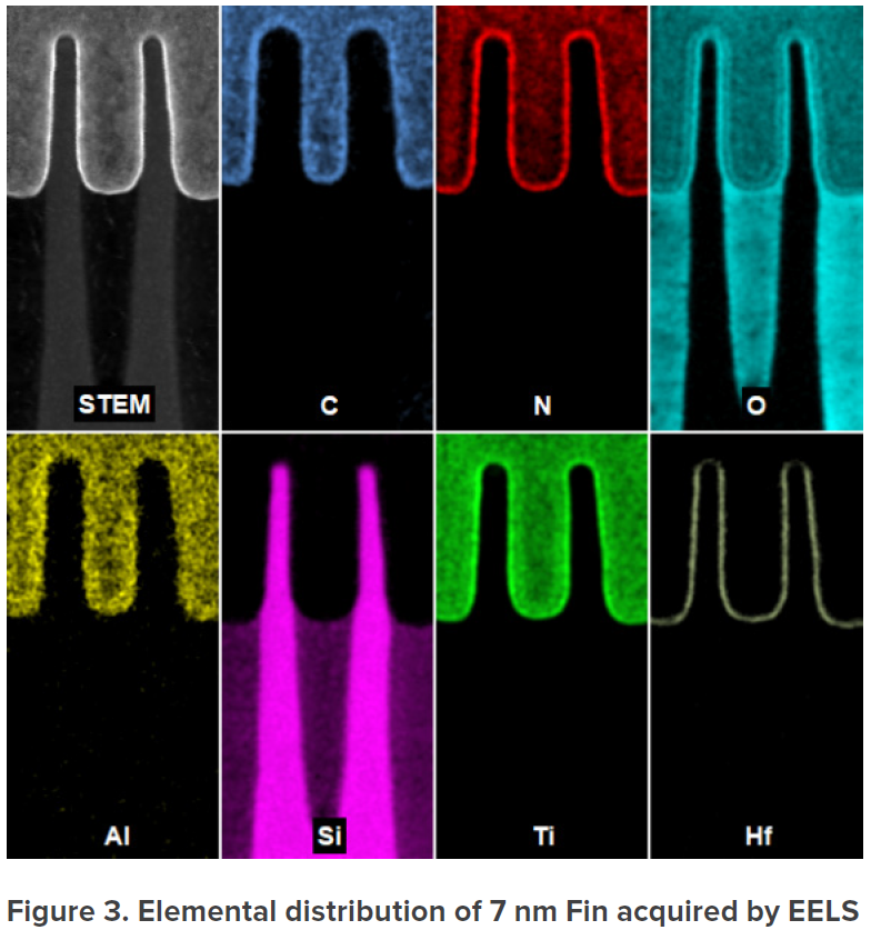
Figure 3 shows elemental distribution of the 7 nm Fin, acquired
by TEM-based EELS (Electron Energy Loss Spectroscopy). Subnanometer layer of high-k dielectric HfOx is seen, similar to that in
22 nm [3]. However, compared to 22 nm Fin, W from metal contact
and Ta in TaN dielectric layer are missing.
Download the App Note for more information on the study of FinFET technology
Would you like to learn more about the analysis of FinFET's?
Contact us today for your FinFet analysis needs. Please complete the form below to have an EAG expert contact you.