Home » Atomic-Resolution Secondary Electron Imaging
AC-STEM with Secondary Electron (SE) imaging provides the unique capability of evaluating specimen surface morphology with atomic-resolution.
Aberration Corrected Scanning Transmission Electron Microscopy (AC-STEM) is now widely used in material science research, product process control, and device failure analysis for a wide variety of different materials. The aberration-corrected electron probe scanned across a thin specimen provides atomic-resolution imaging not only from transmitted electrons (TE – HAADF, BF, ABF…), but also from secondary electrons (SE) emitted from the surface of the specimen. AC-STEM SE imaging provides a unique method of characterizing material structure including important depth information.
When surface information of a thin specimen is desired, STEM SE imaging can be utilized. This includes tasks such as particle morphology, CD measurements, and defect inspection to name a few. In the case of defects, it is often important to understand their location within the thickness of a (S)TEM specimen. Investigations based solely on transmitted electron information can often be inconclusive especially in the case of 3-D structures since TE images only provide a projection of the entire thickness of the sample.
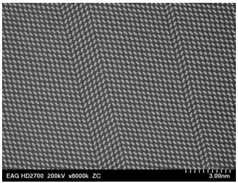
Ultra-high-resolution images at Si twin boundaries
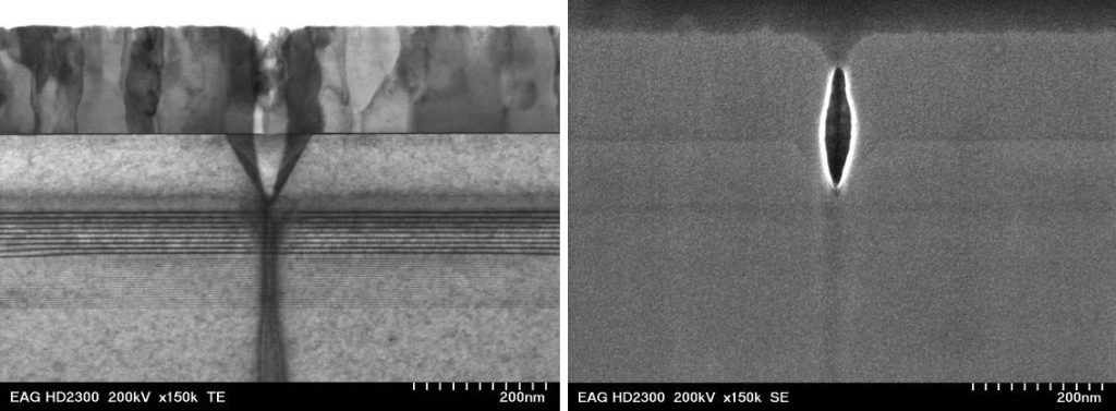
In Figure 1, the BF-STEM (TE mode) image on the left, shows a brighter region above a threading dislocation induced V-defect at the ITO/GaN EPI interface. This contrast is indicative of a region having lower average Z, but it is impossible to distinguish whether the feature is simply filled with lighter material such as Carbon or is a void. However, SE imaging provides the conclusive answer.
Figure 1: BF-STEM and SE images of voiding metal/EPI interface above a threading dislocation. Left: BF-STEM in TE mode; right: STEM-SE mode
Would you like to learn more about Atomic-Resolution Secondary Electron Imaging?
Contact us today for your Atomic-Resolution Secondary Electron Imaging needs. Please complete the form below to have an EAG expert contact you.
To enable certain features and improve your experience with us, this site stores cookies on your computer.
Please click Continue to provide your authorization and permanently remove this message.