Types of crystal defects that can be observed with TEM
Home » Types of crystal defects that can be observed with TEM
Transmission electron microscopy (TEM) is a Advanced Imaging technique in which an accelerated electron beam is transmitted through a specimen to form an image. A feature of transmission electron microscopy (TEM) is its ability to create images at localized regions within a sample.
A crystal defect occurs when an interruption of the regular geometrical arrangement of atoms creates an imperfection in the material.
Transmission Electron Microscopy is often used to evaluate defects in crystals, but not all defects can be observed with TEM.
For example, defects such as point defects cannot be observed with TEM. This is related to the fact that TEM does not look at every single atom.
Defect types and observability with TEM
Type of defect
Whether it can be seen with TEM or not
Point defect
can not see
Line defect (dislocation)
Visible
edge dislocation, screw dislocation, etc.
Negative
Visible
stacking faults, etc.
Volume defect
Visible (voids, precipitates, etc.)
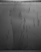
GaN midline defects (dislocations)
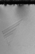
Si surface defects (stacking defects)
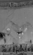
CIGS medium volume defect (void)
Would you like to learn more about crystal defects that can be observed with TEM?
Contact us today for your types of crystal defects that can be observed with TEM. Please complete the form below to have an EAG expert contact you.
To enable certain features and improve your experience with us, this site stores cookies on your computer.
Please click Continue to provide your authorization and permanently remove this message.