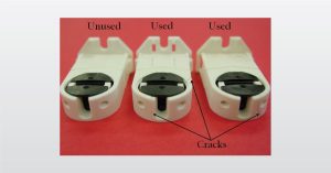
SIMS Characterization of Atomic Layer Deposition in Electronic Applications

Over time, every day technology has continued to advance and evolve. The microelectronics industry has responded with aggressive miniaturization which results in faster and more efficient products. Eventually fundamental physics limits miniaturization, but the demand for computational advancement does not abate. One result is the movement toward three-dimensional transistors (FIN-FET, GAA) and one facilitating technology is Atomic Layer Deposition (ALD).

Atomic Layer Deposition for Thin Films

Atomic Layer Deposition is a vapor phase technique used to deposit thin films onto a substrate. The process of Atomic Layer Deposition involves the surface being exposed to alternating precursors, which do not overlap but instead are introduced sequentially. It is an attractive technique because the Atomic Layer Deposition deposition is conformal as the process is self-limiting and allows for controlled thickness on all surfaces.

Atomic Layer Deposition

As Atomic Layer Deposition is much slower process than traditional Plasma Enhanced Chemical Vapor Deposition (PECVD), sometimes the precursor cycles are reduced whist still providing adequate saturation. Although this increases the deposition rate, it can potentially reduce film quality. 

SIMS Machine

EAG Offers a Wide Range of Techniques for Atomic Layer Deposition

To ensure good Atomic Layer Deposition  film quality, the ALD film structure can be analyzed with Scanning Transmission Electron Microscopy (STEM) and then the film composition can be analyzed with X-ray Photoelectron Spectroscopy (XPS). At Eurofins EAG, we also offer Secondary Ion Mass Spectrometry (SIMS) which can detect any contamination of Atomic Layer Deposition films at ppm to ppt detection limits and can measure interdiffusion between metal and barrier layers. This is particularly important because the contamination in ALD films can affect the performance and reliability of the final product, which is ultimately linked to consumer cost. Likewise, interdiffusion, specifically diffusion of metal contact into the silicon device, can dramatically affect electronic performance.  SIMS is particularly useful for interdiffusion analysis because of its wide range of detection sensitivity. 

EAG continues to be a leader in SIMS analysis and has a team of experts ready to partner with you to produce data driven results. If you’re in the process of working on thin layer films for your next generation electronic devices, please contact us today to learn how EAG can partner with you to analyze your product.

More content you might like...

GC-MS

GC-MS Webinar

In this webinar we will focus on Gas Chromatography-Mass Spectrometry (GC-MS) which allows for the identification of specific molecules

Read More »

To enable certain features and improve your experience with us, this site stores cookies on your computer. Please click Continue to provide your authorization and permanently remove this message.

To find out more, please see our privacy policy.