EAG Analytical Capabilities in Europe Webinar
In this webinar we introduce EAG Analytical Capabilities in Europe at our Eindhoven and Toulouse Laboratories
Home » Benefits of Image Processing
In the world of semiconductors, understanding the materials that are used in semiconductor devices is critical in their performance and reliability. Materials characterization can help provide valuable information to help reduce development time and solve yield problems in semiconductor manufacturing. Electron microscopy techniques play a vital role in semiconductor device characterization, allowing engineers to visually inspect devices and measure critical dimensions relevant to their performance. However, this process can be repetitive and time consuming when done manually.
At Eurofins EAG, we have the capability to generate a large number of measurements in a single image or across a set of images to help customers track critical dimensions and measure material properties such as the layer thickness or surface/interface roughness of a thin film. Statistical analysis allows us to reveal patterns or trends in a large set of measurements that may not be visible when only a limited number of measurements are collected during the analysis. Analyzing the statistics of a large set of measurements increases our confidence that conclusions or correlations drawn from the data are a true reflection of the properties of the whole sample as opposed to only a small section of it.
Image processing is the only practical way to generate enough measurements for the statistics we calculate to be meaningful. A scientist can manually draw a few dozen measurements in a reasonable amount of time, but automatic image processing allows us to collect hundreds or thousands of measurements from the images. In addition, after the initial investment of writing the image processing script, the time necessary to measure additional images is minimal and the measurements are always made with a consistent process.
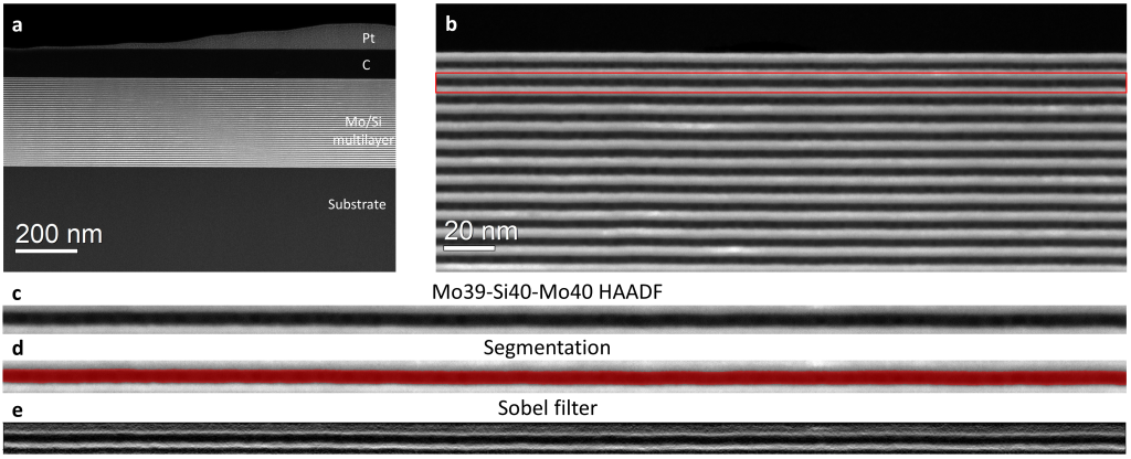
A customer wanted to determine if there was a correlation between the thickness of several layers of a large multi-layer stack (e.g. if a bump in a lower layer might cause a bump in the layers above it). High resolution cross-section images of the multi-layer were collected with an electron microscope. Although a scientist could try to fulfill the client’s request manually by visually identifying bumps and troughs in several locations and making measurements of each layer’s thickness, the process would be slow, tedious, and would yield in only qualitative results.
With image processing, we measured the thickness of each layer at thousands of positions and then used a quantitative method to calculate the strength of the correlation between the layers. The large number of measurements ensures that we’re faithfully capturing the variations in the thickness of each layer and a quantitative comparison unambiguously reveals any correlations present.
Image processing allows us to generate a large set of measurements from an image that would be impossible to do manually. Examining the statistics of these measurements helps to reveal patterns in the data and confidently draw conclusions about the sample’s overall properties.
At Eurofins EAG, our materials and microelectronics services provide valuable insight for semiconductor clients as they develop new processes and materials. Our scientific experts have many years of experience in the semiconductor industry. Contact us today to learn how we can help.

In this webinar we introduce EAG Analytical Capabilities in Europe at our Eindhoven and Toulouse Laboratories
Contamination control and defect reduction are critical issues in the manufacturing process of compound semiconductor devices which can impact the performance of the end product. We can provide valuable insights to identify contaminants and characterize materials throughout the product lifecycle.
Atomic Layer Deposition technology aids in the demand for computational advancement in the microelectronics industry.
In the full webinar we introduce MicroLED Analysis for improved understanding of III-nitride material properties and growth/device processes
To enable certain features and improve your experience with us, this site stores cookies on your computer. Please click Continue to provide your authorization and permanently remove this message.
To find out more, please see our privacy policy.