Comparison between EDS and EELS
Home » Comparison between EDS and EELS
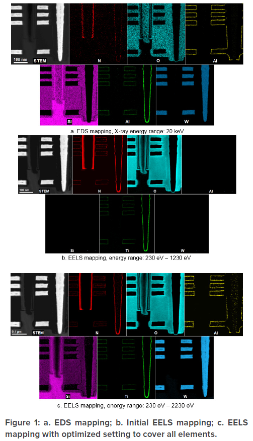
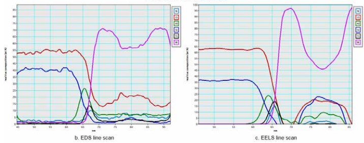
EDS (Energy Dispersive X-ray Spectroscopy) and EELS (Electron Energy Loss Spectroscopy) are elemental analysis techniques integrated with electron microscopes such as TEM (Transmission Electron Microscope). Both techniques provide nanometer-level or atomic-level direct observations and semi-quantitative analysis into materials elemental distribution and concentration, enabling accurate measurement of small complex structures such as FINFET or 3D NAND.
However, the analysis of EDS and EELS require different tool configurations, electron beam settings and analysis approaches. It is often not clear which technique is more appropriate for a certain analysis.
In this application note we compare the respective strengths and limitations of EDS and EELS, by the case studies of a cross-section 3D NAND flash memory sample and a gate-cut FINFET sample. We also show our capability of performing simultaneous EELS and EDS that combines their respective advantages.

Would you like to learn more about EDS and EELS?
Contact us today for your EDS and EELS needs. Please complete the form below to have an EAG expert contact you.
