Failure Analysis of Printed Circuit Boards (PCB)
Home » Failure Analysis of Printed Circuit Boards (PCB)
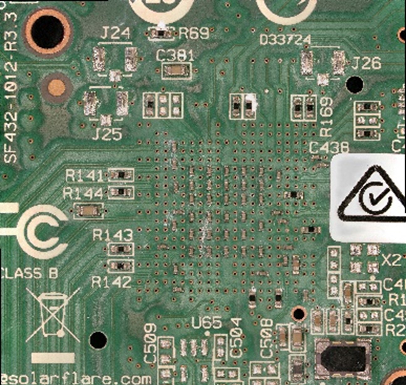
The electronics world depends on a Printed Circuit Board (PCB) to connect devices to systems. There are many assembly steps and materials involved during the assembly of the components on the PCB. All of which can result in electrical issues. There are many techniques that can be utilized to check for issues, defects, and contamination. Failure analysis, materials characterization, reliability testing, and critical dimensions measurements are used to characterize and understand potential problems with PCBs.
PCBs can range from being just a couple of layers to even more complex with 30+ layers. These layers are required to connect discrete devices such as resistors, capacitors, and fuses to the IC devices using solder balls, leads, and pillars. Failures can also occur during the curing process. The complexity of PCBs can result in a high number of potential failure areas.
EAG’s team of failure analysis engineers can enable the understanding of PCB construction, assembly, and materials. With in-depth images and analyses, EAG is able to examine the root cause of failures, critical dimensions, and quality of assembly process. Our experts can assist in PCB improvement resulting in better yields and fewer issues in the field.
Would you like to learn more about the failure analysis of PCB's?
Contact us today for your failure analysis of PCB needs. Please complete the form below to have an EAG expert contact you.