Advances in thin film growth has created a need for characterizing structure and chemistry at the atomic scale. In many cases, features such as interface abruptness and compositional segregation are important for understanding device performance. Scanning transmission electron microscopy (STEM) offers a route towards directly observing material structure on an atom-by-atom basis, however, until recent advances, inabilities to collect enough signal limited high-resolution spectroscopy. At EAG Laboratories, we now have the capability to perform energy dispersive X-ray spectroscopy (EDX / EDS) at the atomic scale.
RESULTS AND DISCUSSION
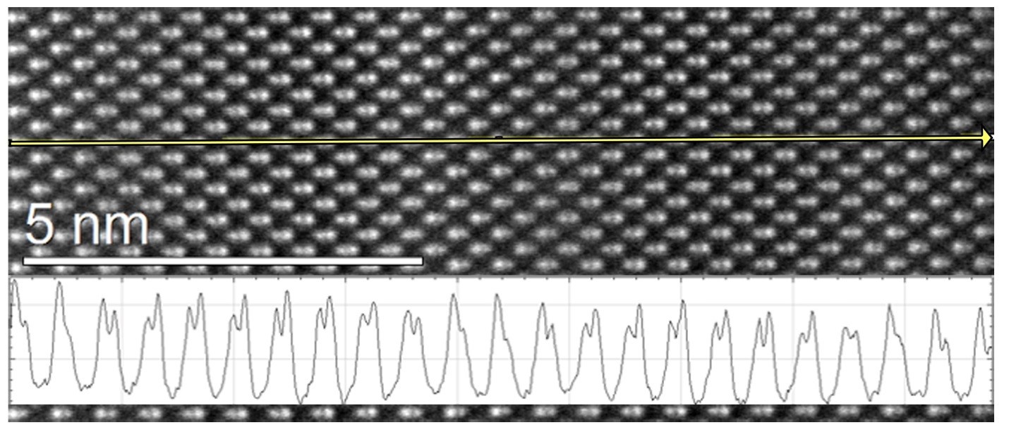
The atomically resolved structure of InGaAsSb superlattice oriented along the <110> zone axis is shown using HAADF (Z-contrast) STEM with an intensity profile corresponding to the yellow line from the image in Figure 1.
Figure 1: HAADF (Z-contrast) image of an InGaAsSb superlattice acquired at atomic resolution. Sample was provided courtesy of North Carolina A&T.
Each bright spot corresponds to the position of a column of atoms with intensity scaling to the average atomic number in the column. Although the intensity scales with atomic number and total number of atoms in a column, extracting compositional information is elusive in many cases. For ternary or quaternary systems, the same intensity for several situations may occur. For example, an In-Ga-Al mixed column may appear to have the same intensity as a pure Ga column.
To resolve ambiguities in HAADF image intensities, spectroscopy can be used to provide maps with signals linked to each elemental species present by using the X-rays generated from the sample-electron beam interaction. In previous generations of EDS detectors, low signal collection hampered the achievable signal at atomic resolution, restricting the ability to perform atomic scale mapping. With modern technology, the attainable signal is roughly an order of magnitude higher and these techniques can now be performed at atomic resolution.
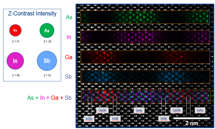
Figure 2 shows an EDS map acquired over a repeat unit of the superlattice structure with colors corresponding to each type of element. In contrast to the HAADF image, each distinct layer is now clearly identified including the interfacial monolayers of InSb, removing the ambiguities associated with the black and white Z-contrast image. As demonstrated through the example in Figure 2, EDS clarifies the layer composition as well as the polarity in the sample. Although the signal is clear for the atomically resolved EDS map, the signal rate is still much lower than the typical Z-contrast image. Thus, EDS mapping can have limited application to samples that are sensitive to extensive electron beam radiation.
Figure 2: Elemental EDS maps for Ga, As, In, and Sb overlaid on the HAADF (Z-contrast) image. Sample was provided courtesy of North Carolina A&T.
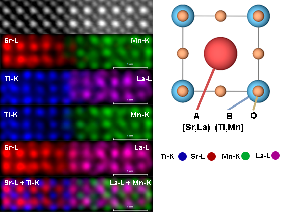
Figure 3: EDS map resolving the atomic structure across an STO/LSMO interface with different combined elemental maps on the left side and a schematic showing the perovskite crystal structure on the right.
For more complex structures with unique lattice sites, atomic resolution can be employed to determine where each type of atom resides in the crystal. Take for example, strontium titanate (STO) and lanthanum strontium manganate (LSMO) both belong to the perovskite (ABO3) structure, a cubic system with different elements occupying the A and B sublattices. Figure 3 shows the atomically resolved elemental signal for the cations at the STO/LSMO interface. By comparing the signals from the second panel (Sr + Mn) and third panel (Ti + La), we observe that the La and Ti species form the interfacial layer and that there is a deficiency of signal in the Sr and Mn. Panels 3 and 4 show the signal for the A and B sites across the two layers where La replaces Sr in the A sublattice and Mn replaces Ti in the B sublattice. Finally, we can form a composite map showing the elemental distribution across the interface.
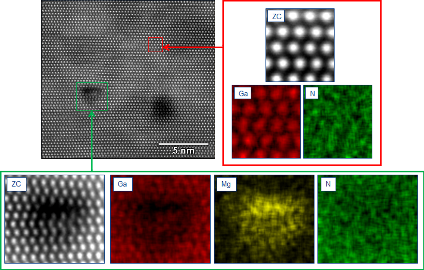
Figure 4: Atomically resolved HAADF image and EDS maps showing the bulk GaN crystal and a Mg containing defect. Sample was provided courtesy of Hosei University Research Center of Ion Beam Technology.
In many atomic scale defects results in chemical segregation. For the example of Mg doped GaN, rather than a uniform distribution of Mg throughout the material, defect complexes are formed resulting in dislocations. Figure 4 shows the Mg doped GaN sample with a red box corresponding to bulk GaN and the green box indicating the lattice defect. Using atomically resolved EDS, the defect is shown to be rich in Mg and deficient in Ga. Without a spectroscopic fingerprint, determining the distribution of Mg in the sample would not be possible through standard Z-contrast imaging.
Outside of the examples shown, this technique is broadly applicable to crystalline materials. Several specific examples can be found through the references at the end of this article. In many cases, crystalline lattices have unique sites which certain elements preferentially reside in the structure. The distribution of elements in the lattice is fundamentally linked to the properties and can affect areas of interest such as interfaces.
Would you like to learn more about Atomic Resolution EDS?
Contact us today for your Atomic Resolution EDS needs. Please complete the form below to have an EAG expert contact you.
To enable certain features and improve your experience with us, this site stores cookies on your computer.
Please click Continue to provide your authorization and permanently remove this message.