Until recently, organic analysis using techniques such as X-ray Photoelectron Spectroscopy (XPS) or Time-of-Flight Secondary Ion Mass Spectrometry (TOF-SIMS) has been limited to only the outermost surface layers of samples. Chemical state profiling was impossible since the process of traditional inert gas ion sputtering (typically using argon) or other monatomic sputter ions greatly damaged the chemical structure of organic materials, usually to the point where they were no longer recognizable.
Recently, however, new ion guns which allow chemical state profiling have been introduced. EAG Laboratories now has a Buckminsterfullerene (C60, “buckyball”) ion gun specifically for sputter etching polymers and other organic materials.
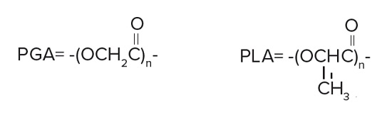
Bioabsorbable poly(glycolide) PGA and poly(lactide) PLA
With C60 sputtering we can retain much, if not all, of the chemical structure of sputter etched organics. The applications of C60 sputtering in combination with surface analysis tools include:
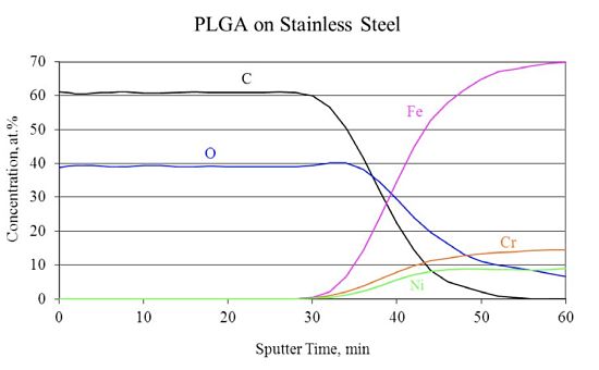
Two examples of the capability of C60 ion bombardment in combination with XPS analysis are shown below. In the first example a few hundred nm thick film of poly(lactic-co-glycolic acid), PLGA, on stainless steel was profiled to demonstrate the excellent retention of chemical state information during the sputter process.
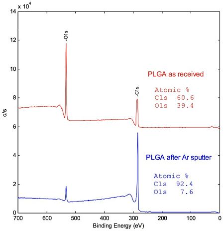
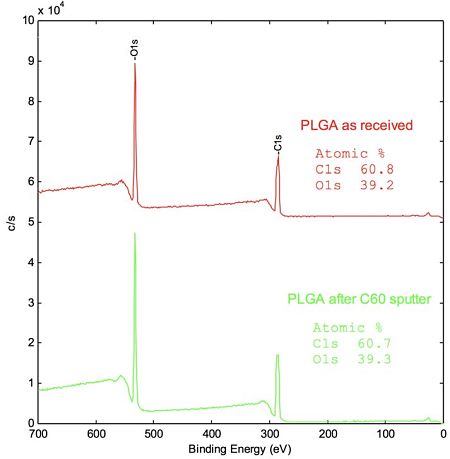
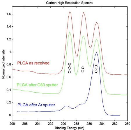
Figures 1 and 2 compare survey scans of PLGA, as received and after sputtering with a standard Ar+ ion beam (Figure 1) and with a C60+ ion beam (Figure 2). The Ar+ ion beam used to sputter PLGA causes a rapid loss in the O signal, which manifests itself as a dramatic change in the C1s region of the spectrum from the polymer (Figure 3). Sputtering with an Ar+ ion beam, shows a dramatic reduction in C-O and O=C-O chemistries and an increase in the C-C signal, as the sample becomes more graphitic in nature. In contrast, Figure 3 also shows that the C region, after C60+ ion bombardment, is almost identical to that of the as-received surface. Figure 4 shows that the intensities of the C and O remain constant throughout the C60+ depth profile through the PLGA.
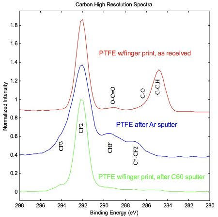
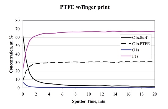
The second example demonstrates the use of the C60+ ion beam as an efficient polymer surface cleaning tool. In this example, a sample of polytetrafluoroethylene, PTFE, was contaminated with fingerprints. As shown in Figure 5, the C1s spectrum of the as-received surface has a strong hydrocarbon line and smaller oxidized C components, in addition to the expected CF2 line, consistent with PTFE. An attempt to clean off the contamination by the Ar+ ion beam removes the hydrocarbon, but severely damages the fluorocarbon chemistry by partially breaking the -(CF2-CF2)n– chain. In contrast, cleaning this surface with the C60+ ion beam causes almost no damage. The depth profile in Figure 6, plotting two types of carbon (surface hydrocarbon and PTFE) shows the efficiency of contamination removal by the C60+ ion beam and the retention of the structurally significant CF2 signal.
These examples illustrate the excellent prospects for using C60 depth profiling and surface cleaning to analyze samples that would be very difficult to tackle using traditional monatomic sputtering.
Figure 1 Survey spectra of PLGA, as received and after Ar+ sputter.
Figure 2 Survey spectra of PLGA, as received and after C60+ sputter.
Figure 3 C1s High resolution spectra of PLGA, as received, after Ar+ sputter, and after C60+ sputter.
Figure 4 C60+ sputter depth profile of PLGA deposited on SST substrate.
Figure 5 C1s High resolution spectra showing the removal of finger print contamination from PTFE surface: as received – contaminated, after Ar+ sputter – damaged, and after C60+ sputter – cleaned.
Figure 6 C60+ sputter depth profile showing the removal of finger print contamination from PTFE surface.
Would you like to learn more about XPS Analysis with C60 Sputtering?
Contact us today for your XPS analysis with C60 sputtering. Please complete the form below to have an EAG expert contact you.
To enable certain features and improve your experience with us, this site stores cookies on your computer.
Please click Continue to provide your authorization and permanently remove this message.