Characterization of Surface Contamination
Home » Characterization of Surface Contamination
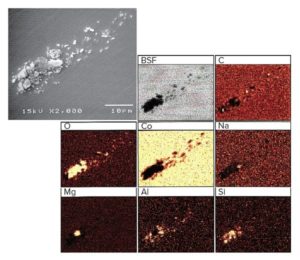
Elemental characterization of defects and contamination on surfaces is a necessity for failure analysis. Energy Dispersive X-Ray Spectrometry (EDS), combined with Scanning Electron Microscopy (SEM) provides a rapid and efficient tool for characterizing particles and defects which are on the order of 1µm or larger. Modern instruments allow for the detection of light elements (B through F), as well as the higher Z elements, and for simultaneous imaging of multiple elements. The lateral distribution of seven elements is shown in Figure 1 along with secondary electron and back-scattered electron images. From this collection of images it is readily determined that the contamination is a conglomeration of carbon bearing material and oxides of Mg, Al and Si.
Figure 1 shows Secondary Electron Image (SEI) of the surface defect and associated EDS elemental images and back-scattered electron image.
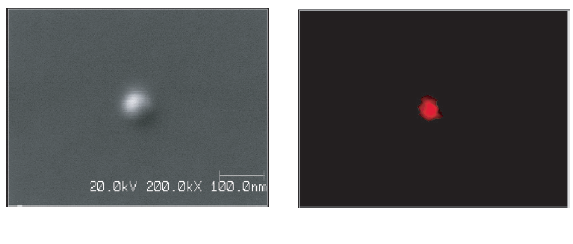
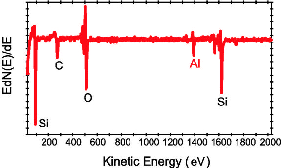
For particles and defects smaller than 1 micron, an ideal tool is Auger Electron Spectroscopy (AES). With this instrument, features as small as 200Å can be characterized elementally. The Auger survey spectrum of a 500Å particle on a silicon wafer reveals the particle contains aluminum.


Would you like to learn more about Characterization of Surface Contamination?
Contact us today for your characterization of surface contamination needs. Please complete the form below to have an EAG expert contact you.