Secondary Ion Mass Spectrometry (SIMS) is an analytical technique that detects very low concentrations of dopants and impurities. It can provide elemental depth profiles over a depth range from a few nanometers to tens of microns.
During fabrication process of GaN on silicon HEMT device, Al and Ga can diffuse into Si substrate. As p-type dopants in Si, Al and Ga can form parasitic conduction channel at Si interface region. Understanding and control of Al and Ga diffusion into Si is important in manufacturing high performance GaN/Si HEMT devices.
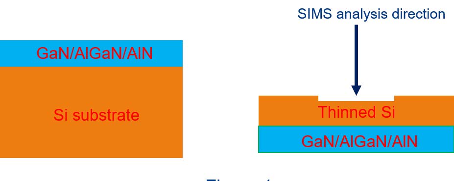
SIMS analysis from Si side has been used to study the diffusion of Al and Ga.
Combined with parallel polishing, SIMS depth profile from Si side is a great tool to understand Al and Ga diffusion into Si for GaN/Si HEMT structure. If remaining Si thickness is greater than ~ 3 μm, sputtering induced roughness can results artificial tails at Si interface region.
Would you like to learn more about SIMS Analysis of Al and Ga Diffusion?
Contact us today for your SIMS analysis of Al and Ga diffusion needs. Please complete the form below to have an EAG expert contact you.
To enable certain features and improve your experience with us, this site stores cookies on your computer.
Please click Continue to provide your authorization and permanently remove this message.