Atom-By-Atom Distance Measurements
Home » Atom-By-Atom Distance Measurements
Knowledge of the precise position of atom columns provides access to measuring global and local lattice parameters, strain analysis, and quantitative investigation of lattice changes near defects, interfaces, and secondary phases.
Tailoring device performance now requires strict control of materials behavior at the atomic scale. The need for such localized control has necessitated new breakthroughs in characterization to be able to understand the structure at an atom-by-atom basis. Aberration corrected scanning transmission electron microscopy (AC-STEM) has enabled the analysis of atomic structure and composition to become routine. One area that has remained challenging to study at the atomic scale is precise atomic spacing or strain measurements. In this application note, we show the possibility to extract distance information at an atom-column to atom-column basis with picometer level precision. We demonstrate how atom columns can be identified and their positions fit. Knowledge of the precise position of atom columns provides access to measuring global and local lattice parameters, strain analysis, and quantitative investigation of lattice changes near defects, interfaces, and secondary phases.
The figure to the upper right shows a frame averaged HAADF STEM image of quantum wells in a GaN-based LED. The thin bright layers are InGaN, while the dim, thicker layers are nominally pure GaN. Download the application note to learn more.
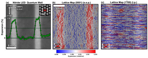
(a) Frame averaged HAADF STEM image including a portion of the quantum well region in a nitride-based light emitting diode. Relevant inter-planar spacings and indicated by the magnified inset. The out-of-plane lattice expansion is overlaid on the HAADF image in green. (b-c) show the out-of-plane and in-plane atom column distance maps respectively.
Would you like to learn more about AC-STEM?
Contact us today for your AC-STEM needs. Please complete the form below to have an EAG expert contact you.