What is the relationship between Auger analysis and EDS analysis?
Home » What is the relationship between Auger analysis and EDS analysis?
Both Auger Electron Spectroscopy (AES) and Energy Dispersive X-ray Spectroscopy (EDX / EDS) are used for elemental analysis of small localized regions by exposing the sample to a focused electron beam. Although both are very useful techniques, the type of signal detected is different, and the information depth of each measurement is quite different.
Since AES is reliant on the detection and measurement of only Auger electrons, the information depth is determined by the depth from which Auger electrons can escape the sample. This distance is very short so the information depth is limited to about 10 nm or less from the sample surface.
Since the escape depth of Auger electrons is low, it is possible to obtain the depth distribution of elements of interest by sputtering the sample with an ion gun (e.g. Ar+) and obtaining Auger spectra alternately in between sputter steps. In contrast to Auger analysis, EDS analysis involves the detection and measurement of X-rays that are characteristic of the species present. The depth of escape of these X-rays is about 1um, which is more than 100 times deeper than the Auger electron escape depth. Please note that the EDS information depth is variable, particularly with respect to the electron beam energy.
Auger analysis is generally more suitable than EDS analysis for the analysis of very thing surface layersd, particles or contaminants, e.g. 50 nm thick, or less. If EDS was used for such an analysis, it is very likely that the spectra obtained would contain more information from beneath the surface layer or feature of interest, rather than from the surface of the sample itself. This convolution of surface information with intense signal from beneath the surface makes it difficult to fully and unambiguously identify thin surface contaminants, particles or layers. As a general guideline, EDS is most suitable for measuring foreign matter and local areas of 0.5um thickness or greater.
When an EDS detector is mounted on a TEM device, the sample is usually sliced to a thickness of 100 nm or less for TEM measurement. Because the sample is so thin, there is just empty space in the volume where the most intense X-rays would come from in a bulk sample. Thus, TEM-EDS does not depend on the characteristic X-ray escape depth as in SEM-EDS. The thickness of the sample is effectively the information depth. This is because the thickness of the TEM sample is less than the characteristic X-ray escape depth.
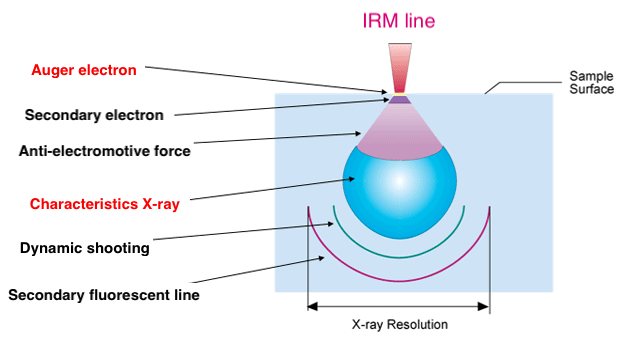
Difference in depth of various signals obtained from interaction between incident electrons and sample
In Auger analysis for, an information depth of about 10 nm or less can be obtained from a small spot irradiated with the incident electron beam. On the other hand, in EDS analysis, the characteristic X-rays come from a much large volume, that depends on the acceleration energy of the electron beam. The information comes from a much larger volume (about 1um3) than the irradiated spot that the X-ray actually hits. This can be an advantage for EDS in some cases (particle/layer/feature sizes of 0.5um or larger) and an advantage for Auger in other cases (smaller features and thin films).
Observation of a particle and elemental analysis by SEM-EDS
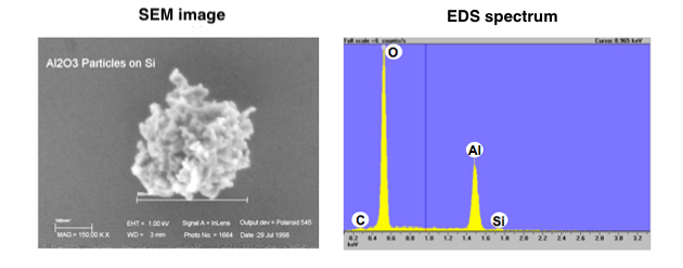
SEM image and EDS spectrum (using a low energy 3 keV electron beam) of 0.3um Al particles on Si substrate. It can be seen that the foreign material is composed of Al and O.
In normal EDS analysis, particles with a size of 0.5um or more are targeted.
Analysis of a particle and element mapping on a hard disk by Auger
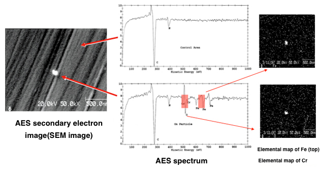
Analysis of a particle with a size of about 100nm. It can be seen that the particle is composed of Cr and Fe.In this case, EDS would not be suitable since the small size of the particle would mean a lot of signal would come from the surroundings and not from the particle itself.
Defect analysis of FIB processed cross section using Auger
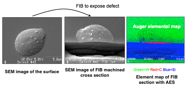
- Si and W were detected from the defect and nearby survey using EDS.
- It turns out that is the particle was C rich in the defective part when analyzed with Auger.
- In EDS, the information depth was too wide and an elemental map showing the C-rich layer could not be obtained.
Defect analysis of FIB processed cross section using Auger
Would you like to learn more about Auger analysis and EDS analysis?
Contact us today for your Auger analysis and EDS analysis needs. Please complete the form below to have an EAG expert contact you.