Scanning Electron Microscopy (SEM)/ Energy Dispersive X-ray Spectroscopy (EDS)
Home » Scanning Electron Microscopy (SEM)/ Energy Dispersive X-ray Spectroscopy (EDS)
SEM coupled with EDS provides high-resolution and high-depth-of-field images of the sample surface along with elemental identification. Scanning Electron Microscopy (SEM) is a widely used technique employed to image the surface of samples. It provides outstanding image resolution, unique image contrast and a large depth of field. Additionally, SEM often requires little sample
preparation and can be coupled with an energy dispersive x-ray spectrometer (EDS or EDX) to provide elemental identification. These attributes make SEM an outstanding choice for imaging applications that require the resolution greater than that provided by optical microscopy, or when there is a need to identify elemental constituents of
micrometer-sized features. Sample preparation methods for SEM are highly developed for the imaging of sub-surface features. Methods include chemical etching, mechanical cross sectioning, planar polishing to remove layers parallel to the surface and ion beam techniques.
A SEM forms an image by rastering a highly focused electron beam, typically with energies of 1 to 20 keV, across a sample and detecting the secondary or backscattered electrons ejected.
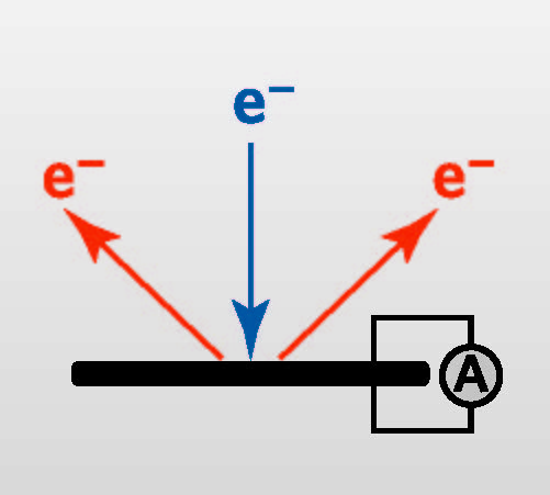
The secondary electrons originate from the top 5-10 nm of the sample and provide information on the topography and, to a lesser extent, on the elemental variation in the sample. Backscattered electrons escape from deeper within the sample and provide information chiefly on the average atomic number of the sample. The incident electron beam, when imparting energy to the sample, can cause emission of x-rays that are characteristic of the sample atoms. The energies of the x-rays are characterized using EDS and can be used to identify the elements in the sample. EDS is primarily a qualitative technique providing data from about a micrometer in diameter and a micrometer deep.
Strengths
- Rapid, high-resolution imaging
- Quick identification of elements present
- Excellent depth of field
Versatile platform that supports many other
tools
Limitations
- Vacuum compatibility typically required
- SEM may spoil sample for subsequent analyses
- Ultimate resolution is a strong function of the sample and preparation
- Insulating samples may need to be coated
Common Applications
- Failure analysis of integrated circuits
- Process development of submicron films
and features for optics, photovoltaic, semiconductor, biotechnology and other industries - Characterization of metal corrosion
- Elemental ID of particles and process residues
- Investigation of interfacial layers, oxidization
and contamination - Imaging of surface topography, including pits,
scratches and bumps
EAG has more than 25 SEM systems in the network, including: high resolution field emission tools, high voltage tools (30 keV in SEM and 200 keV in STEM), tools that can operate in “Environmental” mode (they operate at a higher vacuum pressure than a typical SEM), tools that can accommodate 300 mm wafers and more than 15 focused ion beam-SEMs (Dual Beams). We have a very wide range of sample preparation capability using mechanical and various ion beam methods.
Besides our extensive hardware collection, EAG has over 25 people who work on SEMs regularly, with experience ranging from Ph.D.’s to FAB process managers, to experts in metallurgy. Our labs service industries such as semiconductor, medical device, optics, energy storage, cell phones, piping and printing. Contact us to learn how we can help you on your next project.
Would you like to learn more about SEM EDS?
Contact us today for your SEM EDS needs. Please complete the form below to have an EAG expert contact you.