Identification of Interface Contamination Using Auger Electron Spectroscopy (AES)
Home » Identification of Interface Contamination Using Auger Electron Spectroscopy (AES)
Identification and elimination of interface contaminants is critical for successful production and the ultimate performance of semiconductor devices. Interface contaminants include, but are not limited to, organic and inorganic cleaning residues, residual etch stops, metals, and deposition chamber contaminants. In order to detect interface contamination on patterned devices an analytical technique must have good spatial resolution and good sensitivity for a wide range of elements. Numerous techniques are suitable for devices with features greater than ~50μm x 50μm. For features smaller than 1μm, Auger Electron Spectroscopy (AES) is the technique of choice for analyzing interfacial contaminants.
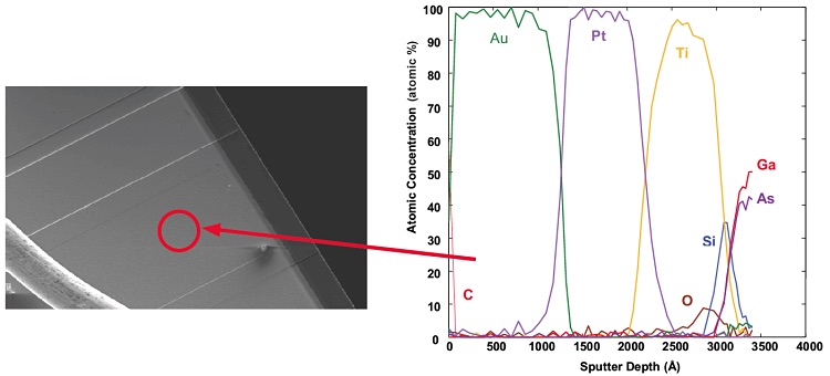
The first example is a laser device that did not meet performance specifications. The facet coating was Au/Pt/Ti on GaAs. The region of interest is approximately 50μm wide and several hundred μm long. An Auger depth profile was acquired from the center of the device as shown in the accompanying secondary electron image. Silicon was detected between the titanium layer and the GaAs substrate. The source of the silicon was identified as a remnant of silicon nitride that was not completely removed prior to the deposition of the titanium. The profile also shows some oxygen present in the titanium layer near the GaAs interface.
Example 1 shows Auger sputter depth profile acquired from a laser semiconductor device shows the presence of silicon at the Ti:GaAs interface. The source of the silicon was residual Si3N4.
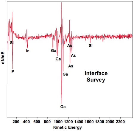
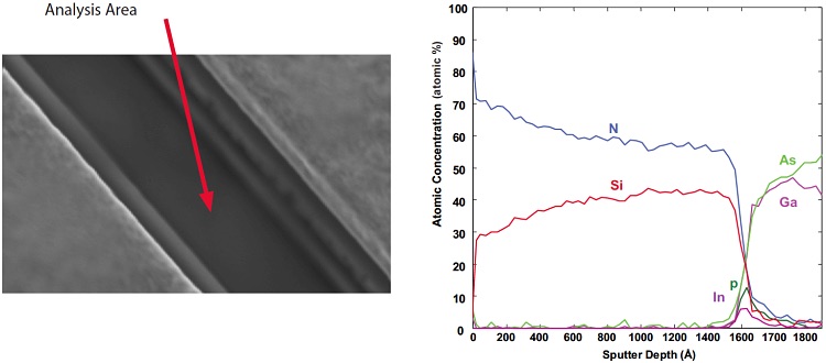
In the second example, the objective of the analysis was to identify contaminants at a silicon nitride-gallium arsenide interface within a 1μm2 area. The depth profile was stopped at the silicon nitride-gallium arsenide interface so that a survey spectrum could be acquired. The profile and interface survey spectrum revealed the presence of indium and phosphorous at the interface. The contamination was identified as residual InGaP which was used as an etch stop layer that was not completely removed during wafer processing.
Example 2 shows Auger sputter depth profile acquired from a 1μm2 area shows the presence of indium and phosphorous at the Si3N4:GaAs interface. The contamination was identified as residual InGaP etch stop.
Would you like to learn more about Identification of Interface Contamination?
Contact us today for your identification of interface contamination using AES. Please complete the form below to have an EAG expert contact you.