Scanning Capacitance Microscopy (SCM) of a Power MOSFET
Home » Scanning Capacitance Microscopy (SCM) of a Power MOSFET
SCM provides doped region distribution mapping, profiling and dimensional analysis for the research and development, failure analysis and quality control of electronic components.
Progress in technology largely depends on the continued miniaturization of electronic components. Smaller components will enable increased switching speeds and device densities for faster computing, larger memory capacity, and improved digital image quality. The current state-of-the-art devices are already below 10nm in size. Characterizing these devices is becoming increasingly challenging because some traditional techniques do not have the required spatial resolution to address such small structures. An alternative method to study these devices is Scanning Capacitance Microscopy (SCM), an AFM-based technique. SCM produces maps of the distribution of electrically active carriers in semiconductors with high lateral resolution.
In this application note, a commercially available power Metal-Oxide-Semiconductor Field-Effect Transistor (MOSFET) was analyzed using SCM. Power MOSFETs are common power devices used in many applications such as consumer electronics, automotive electronics, power supplies, voltage converters, and battery chargers. Download the application note to learn more.
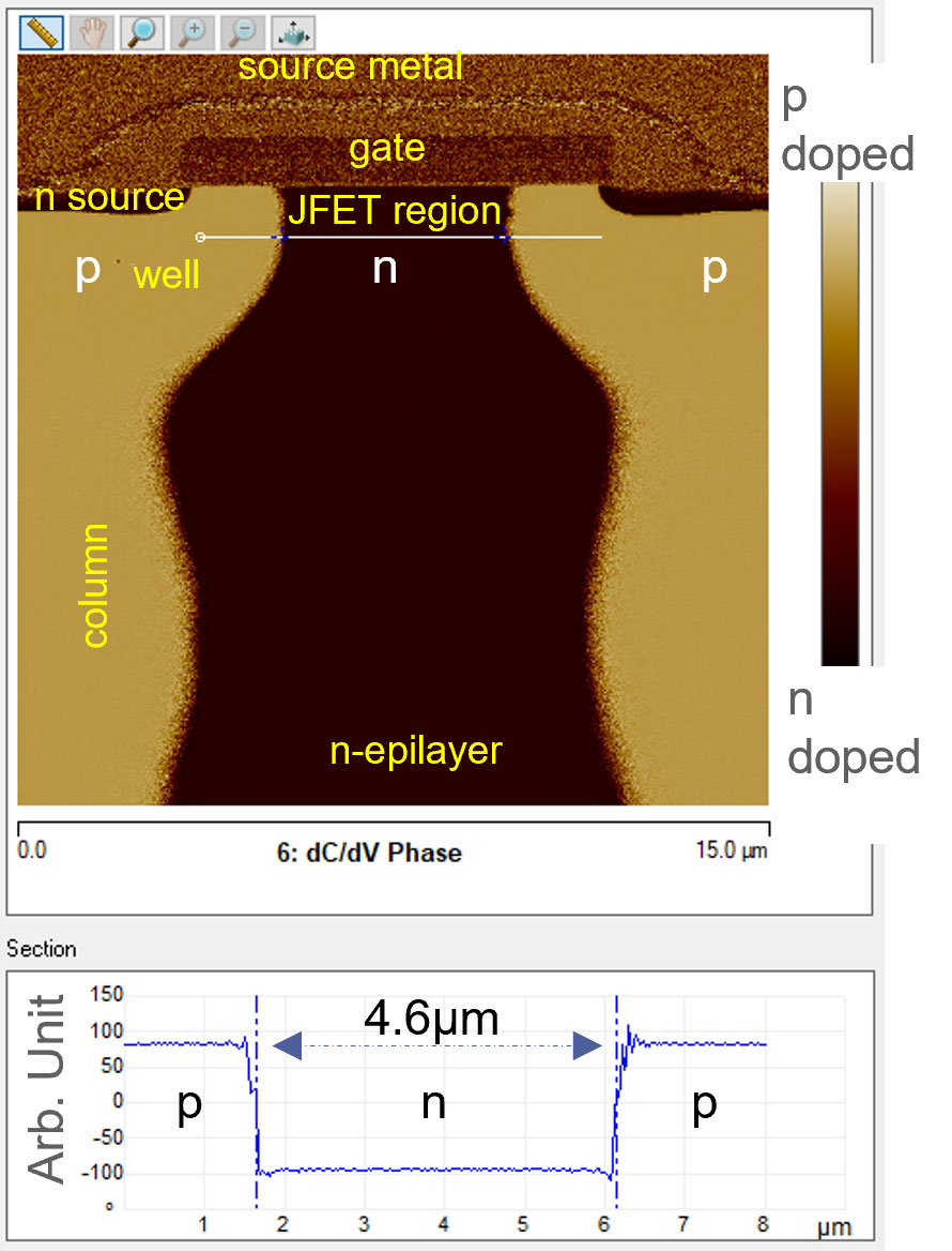
SCM image of the cross sectioned Power MOSFET.
Top image – dC/dV phase (dopant type) image (15µm x 15µm). Bottom image – The blue trace is the dC/dV phase line profile (relative doping type) along the white horizonal line in the phase image on the top.
Would you like to learn more about SCM?
Contact us today for your needs. Please complete the form below to have an EAG expert contact you.