CdTe Thin Film PV – Application Discussion
Home » CdTe Thin Film PV – Application Discussion
CdTe thin film PV is one of the main thin film PV technologies being commercialized. CdTe has the advantage of a direct bandgap which matches well with the solar spectrum, a high absorption coefficient, the ability to be doped both n-type and p-type, and processes that can work for low cost, large scale manufacturing.
The main areas for improvement of CdTe thin film PV are the cell and module efficiencies. Materials characterization using surface analysis methods can be used to support R&D of efficiency improvements.
The representative schematic of the CdTe Thin Film PV device structure shown in Figure 1 illustrates some of the ways surface analysis can help.
On the left side of the schematic we see the layered structure. The light enters through the glass substrate (bottom of the schematic), through the TCO (transparent conducting oxide), the thin (50-150 nm) CdS film, and is absorbed in the thicker (2-8µm) CdTe layer where electron-hole pairs are formed.
The p/n junction formed by the CdS/CdTe heterojunction creates a depletion region which separates the electron and holes which are then collected by the TCO and the metal contact formed on the CdTe surface. The CdS and CdTe layers are made up of multi-crystalline grains resulting in textured or rough interfaces. Thermal processing can cause diffusion between layers (e.g., S) or introduce new elements (e.g. Cl from a Cl-containing anneal step, Cu from the metal contact) that may or may not be detrimental to device performance. The metal contact and its interface with the CdTe are especially sensitive to the surface chemistry of the CdTe before the metal contact is added. In addition there are a wide range of possible materials used for the metal contact, for the TCO, and for doping the CdTe, all of which might be used to improve the device efficiency.
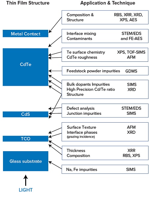
On the right side of the schematic we see that if a soda lime glass is used for the glass substrate, impurities such as Na or Fe may diffuse into the device. This impurity diffusion can be measured by SIMS.
The glass substrate has a TCO layer, such as SnO2:F, ITO (In2O3:Sn), or ZnO:Al between the substrate surface and the CdS layer. The TCO may include a high resistivity buffer layer, such as an oxide like SnO2, In2O3, Ga2O3, ITO, or ZnO. The phase of this material can be measured with XRD and the thickness can be measured with XRR. The composition of these layers can be measured with a variety of techniques, such as RBS and XPS. Phase or composition changes of these layers due to accelerated environmental tests can also be determined with these techniques. Surface texture of the TCO before CdS deposition can be measured with AFM.
The thin CdS layer is normally deposited by a chemical bath step. Phases, composition and thickness, as well as impurities can be determined by XRD, XPS, RBS, XRR, and SIMS. Surface texture can be measured with AFM. Defects can be analyzed by STEM/EDS.
The thick CdTe layer is deposited by a variety of methods, but in all cases is a multi-grain structure. GDMS can be used to quantitatively measure impurities in the CdTe feedstock powder or granules. GDMS can also measure the impurities in Cd and Te feedstock. These impurities can include unwanted counter dopants, and elements that cause electron-hole recombination in the depletion region, or elements that can contribute to structural defects that interfere with current collection. The Cl-containing thermal treatment changes the grain structure. XRD can determine the structural phases of the CdTe and CdS before or after thermal treatment. SEM and TEM can provide structural information about the CdTe/CdS interface before and after the thermal treatment. SIMS can provide quantitative measurement of dopants and impurities in the CdTe layer. Because the CdTe surface is rough (textured), the accuracy of the SIMS profiles can be improved by a polish of the CdTe surface before obtaining the SIMS profile. This also helps in measuring the S diffusion profile from the CdS into the CdTe. The surface texture of the CdTe layer before forming the metal contact can be measured by AFM. The surface chemistry (e.g., Te bonding) of the CdTe before metal contact can be measured by XPS, and TOF-SIMS can provide surface chemistry as well.
The metal contact normally contains Cu which diffuses into the device. The amount of Cu and its location in the device can either be beneficial or detrimental to device performance. The Cu profile can be measured by SIMS through the device. The interface between the metal contact and the CdTe can be analyzed by STEM/EDS and FE-AES (for a profile through a single CdTe grain). There are a variety of approaches to the contact, including for example, Cu-doped graphite paste, Cu/Au, Cu/Mo, Cu/ITO, and ZnTe:Cu. Composition, thickness, and phases of the metal contact can be analyzed by a variety of techniques, such as RBS, XRR, XRD, XPS, and AES.
For the module there is usually some kind of encapsulation material used and this can be analyzed by GCMS and FTIR.
Would you like to learn more about CdTe Thin Film PV analysis?
Contact us today for your CdTe Thin Film PV needs. Please complete the form below to have an EAG expert contact you.